Page 1 of 6
Advice needed on SBC
Posted: Thu Jul 26, 2018 4:17 am
by Floopy
I asked this in the Denial forum (vic-20) and I was told that I could find people who would be up to the task here.
SBC (single board computer)
A quick introduction. My name is Floopy, (not really) I study mechanical engineering, but electronics is a hobby. I've been messing around with the Commodore line of computers for almost two years now and I've been hooked ever since.
I don't have any classes which means I can finally get working on projects. I have wanted to build a 6502 single board computer for a while now. I have managed to pull together a (hopefully) working schematic. I would like to ask if anybody can let me know what should be changed, what should be added and what could be improved. The only electronics course I have ever taken was about oscilloscopes and how to power light bulbs with batteries. Meaning, that obvious mistakes are prone to happen. Also if this isn't the right board then feel free to move it.
Objective:
Build a experimental computer that can be expanded and re-used for different tasks all based around the 65C02.
Some specifications:
The memory is sectioned into 8 banks each 8192Bytes. I'm using a De-MUX (74138) to do the selecting. It's using the upper 3 bits of addressing.
The main processor is a W65C02, the RAM is a AS6C6264 8kx8 bits (8k), the rom is a 27c64.
The "EXP" is expansion. It is for future expansion, the expansion bus carries: clock, D0-D7, A0-A15, R/W and a 5V line for small loads.
The crystal is running a 1.000Mz
The current consumption is under 1.5A, so the LM7805 should be enough for the whole board. The voltage input is between 9-12VDC
Notes:
Designed in KiCad, Eagle was too much of a pain to use, tired of running into "upgrade for a bigger area" message.
-Thank you
Re: Advice needed on SBC
Posted: Thu Jul 26, 2018 4:32 am
by BigEd
Welcome floopy!
That's a nice simple minimal design. I think, though, you're going to need at least one logic gate in there too: at present everything is designed on the basis that a clock cycle is an indivisible thing - is either read or write, and selects just one device. But in reality, for ten or twenty nanoseconds after phi2 falls, there is some pushing and shoving as the different signals change from one state to the other. To avoid misbehaviour, the usual thing to do is to use the clock signal itself to distinguish the stable periods towards the end of a cycle from the everything-in-motion periods towards the beginning.
For example, if you explore
Garth's primer, which is well worth some of your time, you'll see this very minimal but safe and working glue design:
(As it happens, we've recently had a couple of related discussions - see
here for example.)
You might well find
Jeff's animated diagrams helpful, or you might want to bookmark them for later.
Edit to add: it's possible the '138 is flexible enough that you can use it to qualify signals with the clock - I haven't thought about that.
Re: Advice needed on SBC
Posted: Thu Jul 26, 2018 4:52 am
by Floopy
Thank you, Garth's primer has been very helpful with this build.
The way I'm understanding it: A sort of way to say to all other devices that it has set everything correctly and then when that is done, give the information it's asking. Is that it?
>That's a nice simple minimal design.
Thank you, it's what I was aiming for. I want to be able to expand it when needed, reason why I have 8 addressing banks (excuse my technical terms). I'm still in fuzzy land when it comes to I/O. I have a few 6530 and 6551 laying in my drawers. I tried making a prototype with perf-board today, but it got too messy. Seeing how the addressing lines are reversed on the Eprom compared to the 6502!
Re: Advice needed on SBC
Posted: Thu Jul 26, 2018 5:03 am
by BigEd
The way I'm understanding it: A sort of way to say to all other devices that it has set everything correctly and then when that is done, give the information it's asking. Is that it?
Yes, that's about right. But note also a possible second problem: one device is accessed, and then another. During the switchover you mightn't want both of them driving the data bus. So, although it's true that the 6502 is deciding who does what (and when) it's not true that the 6502 is the only one talking. It's the only one waving its arms!
Re: Advice needed on SBC
Posted: Thu Jul 26, 2018 5:22 am
by Floopy
Meaning, it might take some time for everybody to stop talking before the information needs to be transferred?
Re: Advice needed on SBC
Posted: Thu Jul 26, 2018 5:27 am
by BigEd
Sleep could be the best idea right now!
Re: Advice needed on SBC
Posted: Thu Jul 26, 2018 6:08 am
by Chromatix
Yes, the 74HC138 has three enable inputs, two inverted (/E1, /E2) and one active-high (E3). So you could feed Phi2 into E3, and the various /CE signals would then be qualified by it.
The propagation time from E3 is the same as from the address inputs, max 35ns at 5V, which is plenty fast enough for 1MHz operation. I would however be cautious of modern 6502s' tendency to change outputs very promptly after the fall of Phi2 (address and data holds are only guaranteed to be 10ns), and this will still be faster than your '138.
So I would at least also qualify your /WE signal separately with a plain logic gate, which will react much faster than the relatively complex '138. The logic term you need is (R/W | ~Phi2); you may be able to obtain ~Phi2 from the Phi1 output of the CPU, so you'll just need an OR gate. And if you're taking Phi1 anyway, you may as well also lead it to the /OE pins of your RAM and ROM.
Re: Advice needed on SBC
Posted: Thu Jul 26, 2018 7:38 am
by GARTHWILSON
Yes, the 74HC138 has three enable inputs, two inverted (/E1, /E2) and one active-high (E3). So you could feed Phi2 into E3, and the various /CE signals would then be qualified by it.
Note however that the 65xx I/O ICs need their select inputs to be true
before φ2 rises, or they won't work. I found out the hard way, decades ago. If you really had to use a '138, you could use two, so one of them would have the φ2 input and the other would not.
My first home-made computer (1985) used a '138; but IMO it gets misapplied a lot.
Re: Advice needed on SBC
Posted: Thu Jul 26, 2018 2:35 pm
by 1024MAK
@Floopy, hello.
With the EPROM, you have the /OE unused. With the chosen SRAM, you have CE2 unused. I point this out, as with these control inputs available, you can use these so that the EPROM and RAM don't become active when the 6502 CPU is not actually driving the address bus with a valid address. The 6502 only puts a valid address on the address bus when Phi2 is high. Then the 74HC138 can stay as it is.
I personally prefer to prevent the EPROM from responding if the CPU attempts to write data to it (as otherwise, briefly both the CPU and the EPROM will both try to drive the data bus lines), but not every one does this.
Mark
Re: Advice needed on SBC
Posted: Thu Jul 26, 2018 2:56 pm
by 8BIT
Welcome Floopy,
One more adjustment, move the EPROM CS from B2 to B8. The RESET, IRQ, and NMI vectors are in the last addressable page, $FFxx, so you need your EPROM to be readable in that range.
Good luck with your project!
Daryl
Re: Advice needed on SBC
Posted: Thu Jul 26, 2018 3:59 pm
by Floopy
Nice to see you here Mark!
Re: Advice needed on SBC
Posted: Thu Jul 26, 2018 4:31 pm
by BigDumbDinosaur
The 6502 only puts a valid address on the address bus when Phi2 is high.
Not so. For best performance, device selection in a 65C02 system should not be qualified by the clock.
 Viewed 8973 times")
- 65C02 Address Setup Timing
If you examine the 65C02 timing diagram and AC characteristics, you'd see that the address bus will become valid
tADS nanoseconds after the
fall of Ø2.
tADS varies to some extent with operating voltage and the Ø2 clock rate, decreasing to a guaranteed value of 30ns at 14 MHz—that is, A0-A15 will be valid no less than 5ns before the rise of Ø2 in a 14 MHz system on five volts.
What should be qualified by Ø2 is read/write access to any non-65xx peripheral hardware, achievable with a circuit similar to the following.
 Viewed 8973 times")
- Qualified Read/Write Generation
In the above circuit,
/RD (read) and
/WD (write) will not be asserted unless Ø2 is high, which is when the contents of
D0-D7 are guaranteed to be valid.
65xx peripheral hardware, such as the 65C22 and 65C51, "knows" about the 65C02 bus cycle and thus accesses to such hardware should not be qualified by anything. All setup for such devices must be completed by the rise of Ø2. Otherwise as Garth noted, it will not work.
Re: Advice needed on SBC
Posted: Thu Jul 26, 2018 5:00 pm
by BigDumbDinosaur
The memory is sectioned into 8 banks each 8192Bytes. I'm using a De-MUX (74138) to do the selecting. It's using the upper 3 bits of addressing.
Why? What is wrong with using linear addressing in a single (larger) SRAM? That 74HC138 won't be doing you any favors with its slow performance. Using a single 32k × 8 SRAM, you can reduce your parts count and you'll gain timing headroom should you later decide to run a faster clock. Take a look at Alliance's AS7C256B-15PIN 32k × 8 SRAM, which is in a DIP28 package and has a 15ns access time.
The "EXP" is expansion. It is for future expansion, the expansion bus carries: clock, D0-D7, A0-A15, R/W and a 5V line for small loads.
Taking the MPU's buses and signals off-board is not recommended. Garth explains why
right here.
If anything, you should have some I/O built into your unit, such as a 65C22. As it stands, your design has no convenient way to communicate with the outside world.
The current consumption is under 1.5A, so the LM7805 should be enough for the whole board. The voltage input is between 9-12VDC
The current consumption should be but a few hundred milliamps.
Re: Advice needed on SBC
Posted: Thu Jul 26, 2018 5:02 pm
by floobydust
On yet another note, you should look more closely at the expansion connector... you're not bringing any of the signals used for Reset, IRQ or NMI. So if you plan on using some typical I/O devices, you'll likely need these to get them working properly. I would also suggest using something like a DS-1815 Reset chip instead of the RC setup and add a momentary switch as well so you can easily reset the CPU and any other I/O devices.
Good luck with your SBC.
Re: Advice needed on SBC
Posted: Thu Jul 26, 2018 6:58 pm
by GaBuZoMeu
Hi Floopy,
I don't want to sound sarcastic but me thinks your computer is very hard to use: you have no input nor output provided

So far it is just capable of drawing current

(OK, there is
something, but I believe that is not your intention

)
Next your reset circuitry won't work (IMHO). As I see it, C6 pulls /RESET high briefly after power on and is then charged through R2 causing /RESET to see 0V. IOW you need to switch R2 and C6 to have a brief "0" at /RESET and then a "1" during runtime. I would suggest that you add a diode (1N4148 o.e.) parallel to R2 (cathode at +5V). The diode would allow C6 to discharge quickly into Vcc when you turn Vcc off. Otherwise all charge went through /RESET and internal protection diodes into Vcc.
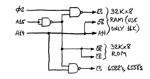
If you use a 74HC139 (instead of your 138) your map would consist of four 16K blocks. Using 8K RAM/EEPROM they would simply appear twice in their 16K block. Using 32K devices you could use just one half (you need to strap the A14 pin of that devices to either GND or Vcc). You had then two 16K regions still available, one for onboard I/O, one for your expansion port. The other half of the 139 can be used to generate a qualified /WR (qualified by PHI2) for your RAM.
Good Luck!