After first power-up, Xilinx ISE 13.4 had successfully seen and programmed 2 selectable FPGA PROMs and the Spartan 6 FPGA itself. I've skipped the hi-frequency bypass cap's because I wish to observe at which point the board fails or the video output becomes noisy. This observation may be at the very beginning of this test, i.e. where a successful video output is generated...
So, I am in need of this real world test to validate my design and before I ask our resident Verilog experts for help, I would like to turn to a Verilog pong project at www.FPGA4FUN.com. It has a very simple video generator that outputs a checkerboard pattern at a resolution of 640x480. The HSYNC and VSYNC part of the code should be OK. However, since I use a videoDAC using 16-bits 5-6-5 RGB and the code was made for 3-bit color using a resistor ladder and signals output from a Spartan 3, it will need a simple modification. Hopefully simple, I will work on this tomorrow...
Once this Test is complete, I'll store the design in the 1st FPGA PROM. Then I'll slightly modify it further, possibly to a different resolution, and store that design in the 2nd FPGA PROM. Once the programmable FPGA PROM selection is verified by jumper and external control pin through the main connector, I will go on to solder-in the SyncRAM. At this point I will surely need help.
It is anticipated that this thread should come to a close at the end of a successful display of 2 simple Video Generator Test 'projects' stored on each of the PROMs, using read-only data from the SyncRAM at a maximum resolution. After this, the real fun begins!
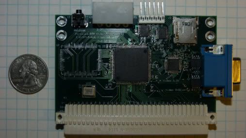
This is the topside of the PVB v1.0g showing the current hardware, true life size if displayed on a 15" 1024x768 monitor. The U.S. quarter is the size 'check', slightly stretched in the horizontal plane due to 16x9 camera settings. I measure that quarter diameter@ 24.11mm with a digital micrometer: