So, bear with me for a moment, this is probably trivial for most of you.
I was working on my board, and this is a somewhat related topic but may be helpful to others, hence a new post.
So I was thinking, to select the various memory address spaces available on the '816 I'd use a few 74 series chips. To that end, from the looks of things the 74 series 74/42 is generally used based on a few schematics I have looked at from various processor boards.
Steve Ciarcia's Build your own computer book, makes it clearer then the various schematics. In his schematic, he has a 74/20 attached with the MREQ, and A13-A15 lines (also on a 74/04), going into the 74/42 with the A10-12 lines. He has A0-A9 giving a 1K address space, and 8 memory bank lines to go to the Chip Selects. This gives a total capacity of 8Kbytes of memory.
So I was thinking, by using A0-A20 gives a 2Mbyte address width per chip. And if I used the 74/20 and 74/42 on A18-A23 I'll get the same 8 memory banks.
Which doing the math gives me a total of 16Mbytes of memory. On 8 selectable groups of up to 2Mbytes. This would work do you think?
Dimitri
Memory Selection ...
-
BigDumbDinosaur

- Posts: 9425
- Joined: 28 May 2009
- Location: Midwestern USA (JB Pritzker’s dystopia)
- Contact:
Re: Memory Selection ...
Dimitri wrote:
So I was thinking, to select the various memory address spaces available on the '816 I'd use a few 74 series chips. To that end, from the looks of things the 74 series 74/42 is generally used based on a few schematics I have looked at from various processor boards.
Steve Ciarcia's Build your own computer book, makes it clearer then the various schematics. In his schematic, he has a 74/20 attached with the MREQ, and A13-A15 lines (also on a 74/04), going into the 74/42 with the A10-12 lines. He has A0-A9 giving a 1K address space, and 8 memory bank lines to go to the Chip Selects. This gives a total capacity of 8Kbytes of memory.
So I was thinking, by using A0-A20 gives a 2Mbyte address width per chip. And if I used the 74/20 and 74/42 on A18-A23 I'll get the same 8 memory banks.
Which doing the math gives me a total of 16Mbytes of memory. On 8 selectable groups of up to 2Mbytes. This would work do you think?
Dimitri
That said, you should consider that Steve Ciarcia's book (Build Your Own Z80 Computer), while an excellent publication in its day, is nearly thirty years old and is geared to an MPU that has relatively little in common with the 65xx family, other than have pins and using electricity. While Ciarcia's book is instructive in a general sense, you may find it somewhat difficult to apply what he presents to a circuit running an 816.
At the time of Ciarcia's book's publication, 74LS logic dominated the computer industry and advances like PLDs were just starting to make the scene (the use of a PLA in the Commodore 64 made that machine's somewhat flexible memory map possible). A lot has changed since then. Some of the gates mentioned in Ciarcia's book are becoming scarce, or are only available in small outline packages that are not particularly hobby-friendly.
In any case, you should consider that doing what you want to do with 74x logic is probably going to torpedo any chances of running your MPU at any significant speeds. If I grasp what you are trying to accomplish, you're going to be using quite a few gates to manipulate the memory map and thus introducing a lot of propagation delay. That sort of logic complexity is better served with a PLD, which can propagate in single digit nanosecond ranges.
I don't know if you are attempting to segment RAM to implement memory protection or not. If this is the case, you might want to investigate setting up RAM in a linear fashion (with space for I/O and ROM, of course) and using the 816's ABORT signal to trap memory access violations or page faults. I can't see doing all that, though, with discrete logic and achieving reasonable performance.
Be that as it may, don't let anything I said discourage you. Go ahead and build a prototype with 74xx logic and then once it seems to be in working order, redesign to use a PLD. Then you can crank up the clock speed.
x86? We ain't got no x86. We don't NEED no stinking x86!
I'm a wrench monkey (Auto shop, Machinist & Mech Design) type, so anything you say is just more knowledge for me to absorb.
His book is indeed old, however being strictly more on the "software" side of things, building hardware is relatively new, especially when you consider this is my first non-microcontroller project and that I'll be using a CPU for the first time.
So I seeked out data sheets on the 8086, 6502, 65816, the 6800 and the Z80, and I've been reading them, there are proprietary chips used (such as 82** or 68** chips) in many examples, and the 74 series logic is used on Prolog's STD boards I got the schematics for. Since Steve mentions it, and shows it the clearest its the reason I decided to use his method as a "basis".
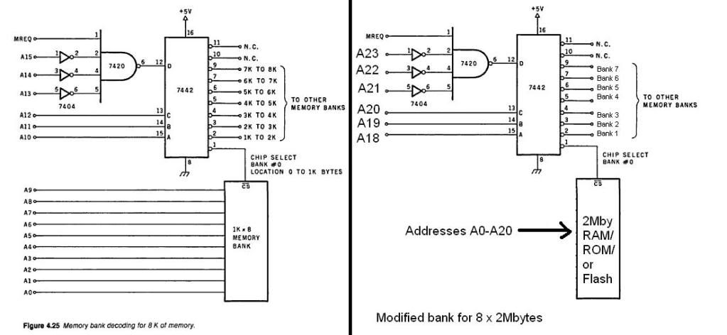
On the left you have the original, but on the right you have the method I was describing.
Dimitri
His book is indeed old, however being strictly more on the "software" side of things, building hardware is relatively new, especially when you consider this is my first non-microcontroller project and that I'll be using a CPU for the first time.
So I seeked out data sheets on the 8086, 6502, 65816, the 6800 and the Z80, and I've been reading them, there are proprietary chips used (such as 82** or 68** chips) in many examples, and the 74 series logic is used on Prolog's STD boards I got the schematics for. Since Steve mentions it, and shows it the clearest its the reason I decided to use his method as a "basis".
On the left you have the original, but on the right you have the method I was describing.
Dimitri
Come to think of it, I don't need the 74/20 I think. I can just wire the upper A21 to A23, which gives me a total of 8 banks anyways using the 74/42 on its own.
Which also solves the issue of using Address lines as direct address lines, and using the same address lines on the converter network.
I feel kinda embarrassed asking this question now.
Dimitri
Which also solves the issue of using Address lines as direct address lines, and using the same address lines on the converter network.
I feel kinda embarrassed asking this question now.
Dimitri
You also need to look at the availability of the chips you use. I had to look for the '42 because its a - for me - unusual IC, and my usual distributor only has them in HCT technology, but not ALS - depends on your choice of technology. You may also not get this IC as SMD, if you would need it.
Besides, even the HCT42 already has a 17ns delay, which is a lot for a current technology (about 2-3 times of other standard ICs). Adding the delay from the '20 (if used) and the address inverter, that limits your maximum clock frequency.
Also, it would be better if you feed the 6502's PHI2 as late as possible into the signal, so the select signal has the shortest delay possible in relation to PHI2, which is _the_ governing signal in a 6502 system.
So for a 1MHz or 2MHz system this schematics might be fine, but going for higher speeds I'd recommend a GAL or CPLD instead
André
fachat wrote:
So for a 1MHz or 2MHz system this schematics might be fine, but going for higher speeds I'd recommend a GAL or CPLD instead
I'll design for it, and once I get the boards made I'll look at picking up a CPLD with a programmer, apparently its only about a 140$ investment if I go the Atmel route with a 44 PLCC package. Which is pretty good I think.
Since I plan on fitting this on the "prototype" size from ExpressPCB which is 3.8 by 2.8 inches at 98$ for them for 3 (or about 32$ each). I think I will use the 44 PLCC package for the 65C816.
Dimitri
I use a Xilinx CPLD with a cheap programmer built from two 74HC125 logic ICs, connected to an "old style" PC printer port ("old style" as in "not connected to something like USB, but be accessible via the PC I/O ports used for the standard printer port(s)"). That setup is even supported by the Xilinx software.
I don't know if that is available for Lattice too, but if so and you have a PC with such a printer port on it, you might want to investigate this direction, should be way cheaper.
André
I don't know if that is available for Lattice too, but if so and you have a PC with such a printer port on it, you might want to investigate this direction, should be way cheaper.
André
-
ElEctric_EyE
- Posts: 3260
- Joined: 02 Mar 2009
- Location: OH, USA
-
GARTHWILSON

- Forum Moderator
- Posts: 8773
- Joined: 30 Aug 2002
- Location: Southern California
- Contact:
Quote:
Come to think of it, I don't need the 74/20 I think. I can just wire the upper A21 to A23, which gives me a total of 8 banks anyways using the 74/42 on its own.
Thank you,
Yes I realized it probably wont work using the lines as decoding lines and as address lines.
However so far my memory map will be:
BA0 - 2MBytes RAM
BA1 - 2MBytes RAM
BA2 - 64KBytes ROM
BA3 - I/O Bus Addresses
BA4 - STD Bus Addresses
BA5 - 2MBytes "User Space" (Flash memory)
BA6 - 2MBytes "User Space" (Flash memory)
BA7 - Reserved For future use (on a 40 Pin header, 21 Address lines, 8 Data lines, and 11 Grounds)
Really I am not using many addresses that can be used this way, and I realize that, however I probably will never use enough memory to matter.
Dimitri
-
GARTHWILSON
- Forum Moderator
- Posts: 8773
- Joined: 30 Aug 2002
- Location: Southern California
- Contact:
Yes, but if you don't have RAM in bank0, I'm not sure if the 65816 will handle that - IIRC you need to have at least the stack there. Plus you have to fiddle with the data bank register upon reset to use RAM in another bank than bank0.
That is one of the most annoying things, that I really don't know why they did the 65816 that way. Why not simply pull RESET vectors from $fffffc instead? In a system where the bank byte is not needed, it would completely be like the 6502, and in other systems you have to take care of 65816 specifics anyway.
With the 65816 pulling RESET from $00fffc you must have - as far as I understand it - a banking scheme in bank 0 to exchange ROM for RAM after boot, or small memory windows (like 32k RAM and 32k ROM). Which makes address decoding (IMHO) unnecessarily complex for a processor being capable of addressing 16M...
Or is there something I don't see?
André
Andre,
Thanks for the tip.
I doubt there is something you don't see, I never worked with a processor so I'm pretty confused over all working backwards, forwards and spinning everywhere as I am trying to digest the data sheets and various schematics of 65C816's on the internet.
I'll use a 32Kbyte RAM unit for the stack (Cypress makes one in a 28 pin SOJ package at 10ns), and a 32Kbyte ROM for the eventual BIOS/OS for the system.
Dimitri