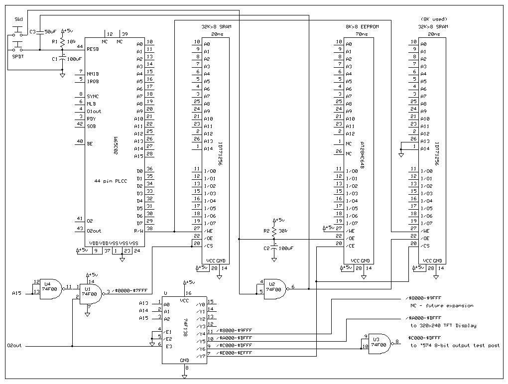
I'm also using a 20 ns 32Kx8 SRAM (lower half of memory) and a 70ns 8Kx8 EEPROM for the OS in my project. Presently, the 65C02 can run up to 7MHz using F series decoding logic (I will switch to AC series soon with supposedly no loss in speed). However I would like to run the OS from SRAM as the access time is 3x faster than the EEPROM, and hopefully I can get the 65C02 up to 12+ MHz.
I've come up with a schematic below which shows the concept of what I am trying to do. I'll try to explain it...
Whenever the EEPROM is accessed, the SRAM on the right is accessed as well. Imagine 2 identical 8Kx8 SRAM's 1 piggybacked on top of the other with all pins touching except the /OE's. When I run the OS copy program, the SRAM will be written to, the EEPROM will ignore writes.
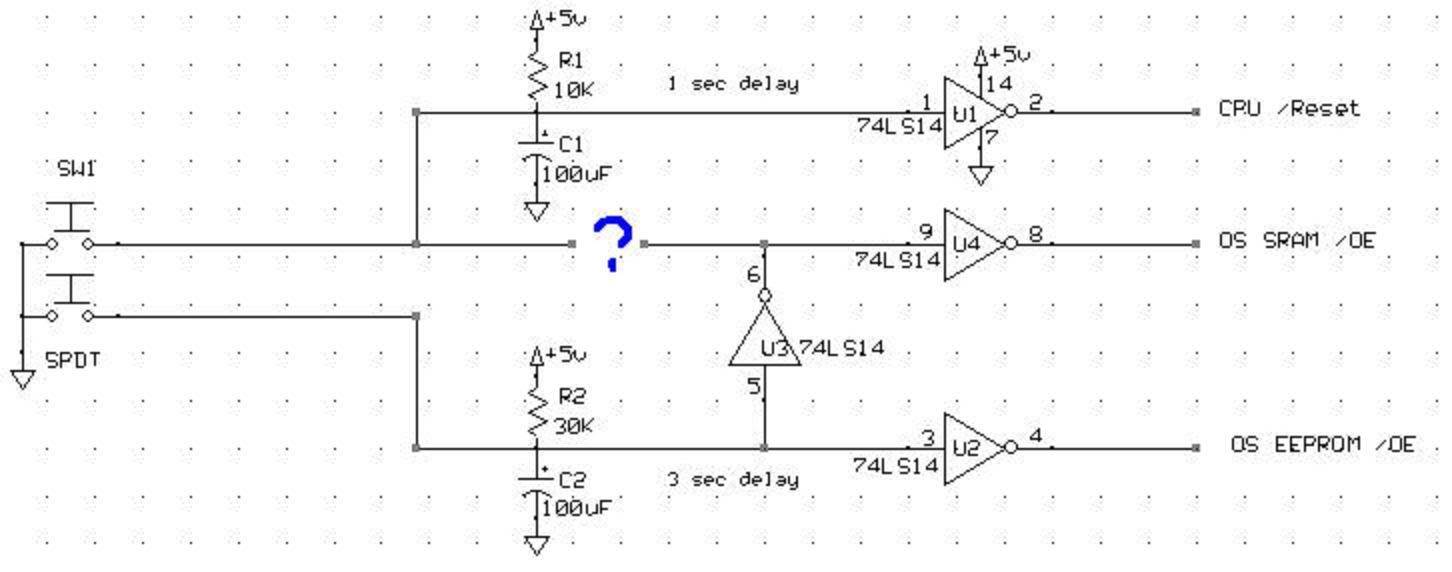
Only the /OE's from the EEPROM and SRAM are manipulated from a signal that originates from a SPDT reset switch.
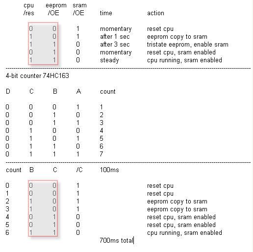
When reset is momentarily pushed, the RC cicuit holds the reset low for approx 1 sec for the CPU, and the /OE of the EEPROM is held low by the second RC circuit for approx 3 sec. This gives the software about 2 sec's to copy the OS to the SRAM, and modify the reset vector to skip over the copy portion of the OS. After the 3 sec's, the signal goes back high, U2 inverts it back to a low signal and it goes into a 50uF bipolar capacitor which is then fed back into the CPU reset thereby resetting the CPU circuit one last time to start the OS running from the SRAM with the new reset vector in place.
I have not wired this up yet and my only anticipated problem is C3, the 50uF capacitor in the upper left. I am not an analog person, and am unsure if this value is right or if the 3 second reset signal will even make it back to the RC circuit that resets the CPU.