Page 7 of 19
Posted: Fri Jan 20, 2012 2:49 pm
by ElEctric_EyE
Yes, this gives us some hope! It is a major part of this project...
The SDRAM physical dimensions I have correct on this board. The only problem I foresee with my design is a potential conflict with the SDRAM controller vs. the pins I have already assigned for the FPGA.
... The block RAMs give 2 areas of 1k for zero page, 4k of stack, 8k intended for 'ROM' and another 16k intended for 'RAM'. (There's enough block RAM for 32k 16-bit words in the LX9.)...
I thought the LX9 had 576Kb(36Kx16) of BlockRAM...So far I have 8K ZeroPage, 4K Stack, and 16K ROM, leaving 8Kx16? for the SDRAM controller. I can trim some to make more available.
Posted: Fri Jan 20, 2012 3:09 pm
by Arlet
The SDRAM physical dimensions I have correct on this board. The only problem I foresee with my design is a potential conflict with the SDRAM controller vs. the pins I have already assigned for the FPGA.
I was going to use my verilog SDRAM controller, not the built-in DDR controller, so it shouldn't really matter what pins are connected. Did you already post a board schematic btw ?
I thought the LX9 had 576Kb(36Kx16) of BlockRAM...So far I have 8K ZeroPage, 4K Stack, and 16K ROM, leaving 8Kx16? for the SDRAM controller. I can trim some to make more available.
My plan was to attach SDRAM directly to CPU bus, and not use any block RAMs for it. If necessary, we can look into adding a cache, but that can be done with as little a one block RAM, up till all of them, depending on priority and application.
Posted: Fri Jan 20, 2012 3:56 pm
by ElEctric_EyE
The schematic I sort of threw together, it's abit difficult to read. I had gotten into the habit of using the Board layout as a schematic. Anyway, I've added them both to the header of this thread. The schematic link is at the very bottom.
Posted: Fri Jan 20, 2012 4:15 pm
by ElEctric_EyE
I just realized the Header pinouts on the schematic will need updating. I'll put some time next few days updating it. The layout is 100% up to date however.
Posted: Fri Jan 20, 2012 4:20 pm
by Arlet
Do you already have a .ucf file with all the FPGA pins defined ?
Posted: Fri Jan 20, 2012 4:29 pm
by ElEctric_EyE
I do. This is just the part defining pin locations. Bottom half is SDRAM:
Code: Select all
NET "MAINCLK1" LOC = P123;			//N_GCLK
//NET "MAINCLK2" LOC = P22;			//P_GCLK
//NET "MAINCLK3" LOC = P51;			//P_GCLK
//NET "MAINCLK4" LOC = P85;			//P_GCLK
//NET "POSC1" LOC = P17;				//P_GCLK
//NET "POSC2" LOC = P50;				//N_GCLK
//NET "POSC3" LOC = P84;				//N_GCLK
NET "VIDEOCLK" LOC = P92;			//N_GCLK
NET "USBCLK" LOC = P24;				//P_GCLK
NET "SCL" LOC = P88;					//P_GCLK RESERVED
NET "SDA" LOC = P87;					//N_GCLK RESERVED
NET "PS2_CLK" LOC = P55;			//P_GCLK
NET "PS2_DAT" LOC = P66;			//RESERVED
NET "SCLK" LOC = P21;				//P_GCLK
NET "MOSI" LOC = P16;				//P_GCLK
NET "MISO" LOC = P23;				//P_GCLK
NET "TX" LOC = P43;
NET "RX" LOC = P40;
NET "O2OUT" LOC = P56;				//N_GCLK	for TFT
NET "WEn" LOC = P59;					//for TFT
NET "A0" LOC = P61;					//for TFT
NET "TFTn" LOC = P67;				//RESERVED for TFT
NET "DataBusOut(7)" LOC = P83;	//for TFT
NET "DataBusOut(6)" LOC = P82;	//for TFT
NET "DataBusOut(5)" LOC = P81;	//for TFT
NET "DataBusOut(4)" LOC = P80;	//for TFT
NET "DataBusOut(3)" LOC = P79;	//for TFT
NET "DataBusOut(2)" LOC = P78;	//for TFT
NET "DataBusOut(1)" LOC = P75;	//for TFT
NET "DataBusOut(0)" LOC = P74;	//for TFT
//NET "PIXDAT(7) LOC = P99;	//RESERVED for CS4954
//NET "PIXDAT(6) LOC = P98;	//RESERVED for CS4954
//NET "PIXDAT(5) LOC = P99;	//RESERVED for CS4954
//NET "PIXDAT(4) LOC = P100;	//RESERVED for CS4954
//NET "PIXDAT(3) LOC = P101;	//RESERVED for CS4954
//NET "PIXDAT(2) LOC = P102;	//RESERVED for CS4954
//NET "PIXDAT(1) LOC = P104;	//RESERVED for CS4954
//NET "PIXDAT(0) LOC = P105;	//RESERVED for CS4954
//NET "SDRA3" LOC = P35;
//NET "SDRA2" LOC = P34;
//NET "SDRA1" LOC = P33;
//NET "SDRA0" LOC = P32;
//NET "SDRA10" LOC = P30;
//NET "SDR1BA1" LOC = P29;
//NET "SDR1BA0" LOC = P27;
//NET "SDR1CSn" LOC = P26;
//NET "SDR1RASn" LOC = P14;
//NET "SDR1CASn" LOC = P12;
//NET "SDR1WEn" LOC = P11;
//NET "SDRA4" LOC = P10;
//NET "SDRA5" LOC = P9;
//NET "SDRA6" LOC = P8;
//NET "SDRA7" LOC = P7;
//NET "SDRA8" LOC = P6;
//NET "SDRA9" LOC = P5;
//NET "SDRA11" LOC = P2;
//NET "SDRA12" LOC = P1;
//NET "SDRCLK" LOC = P15;		//N_GCLK?
//NET "SDRDQM" LOC = P143;
//NET "DQ8" LOC = P142;
//NET "DQ9" LOC = P141;
//NET "DQ10" LOC = P140;
//NET "DQ11" LOC = P139;
//NET "DQ12" LOC = P138;
//NET "DQ13" LOC = P137;
//NET "DQ14" LOC = P121;
//NET "DQ15" LOC = P120;
//NET "DQ0" LOC = P119;
//NET "DQ1" LOC = P118;
//NET "DQ2" LOC = P117;
//NET "DQ3" LOC = P116;
//NET "DQ4" LOC = P115;
//NET "DQ5" LOC = P114;
//NET "DQ6" LOC = P112;
//NET "DQ7" LOC = P111;
Posted: Fri Jan 20, 2012 4:31 pm
by BitWise
I can afford 3 more. 1 ea for Bitwise and TT for their efforts on the 65Org16 assemblers.
Thanks for the thought but I wouldn't have the time to do anything with it and it would just end up collecting dust amongst all the other half finished electronics projects in my house. Keep it for someone who can put it to good use.
Posted: Fri Jan 20, 2012 4:33 pm
by ElEctric_EyE
...Thanks for the thought but I wouldn't have the time to do anything with it and it would just end up collecting dust amongst all the other half finished electronics projects in my house. Keep it for someone who can put it to good use.
Ok, no problem thanks for responding, and Thanks for the As65!
Posted: Sun Jan 22, 2012 9:40 pm
by dclxvi
I've got the next stage of the software portion of the project squared away and ready to go. HESMON, the NMOS 6502 MLM made for the C-64, being readied for the 65Org16. Most likely I will fail, but I look at it like this: I am blazing some trails. Don't get me wrong, I have not tried it yet. It is just that laboring over another's code is just that: a labor, and not necessarily a labor of love. I like to focus on hardware when I tire of it...
I'm not familiar with HESMON specifically, but if you'd like, I can give the 65org16 version of HESMON a try in my 65org16 simulator, or at least look over what you've got so far.
Posted: Mon Jan 23, 2012 12:58 am
by ElEctric_EyE
...I'm not familiar with HESMON specifically, but if you'd like, I can give the 65org16 version of HESMON a try in my 65org16 simulator, or at least look over what you've got so far.
Bruce, Thanks for you interest! As a true 6502 veteran, your opinions hold high value.
I need to actually test what I've converted so far of HESMON...
If you are volunteering to check out my conversion of HESMON, I'd be happy to send the commented version of what I have so far. The JMP's & JSR's are C-64 based.
Posted: Tue Feb 07, 2012 4:13 pm
by ElEctric_EyE
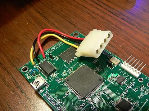
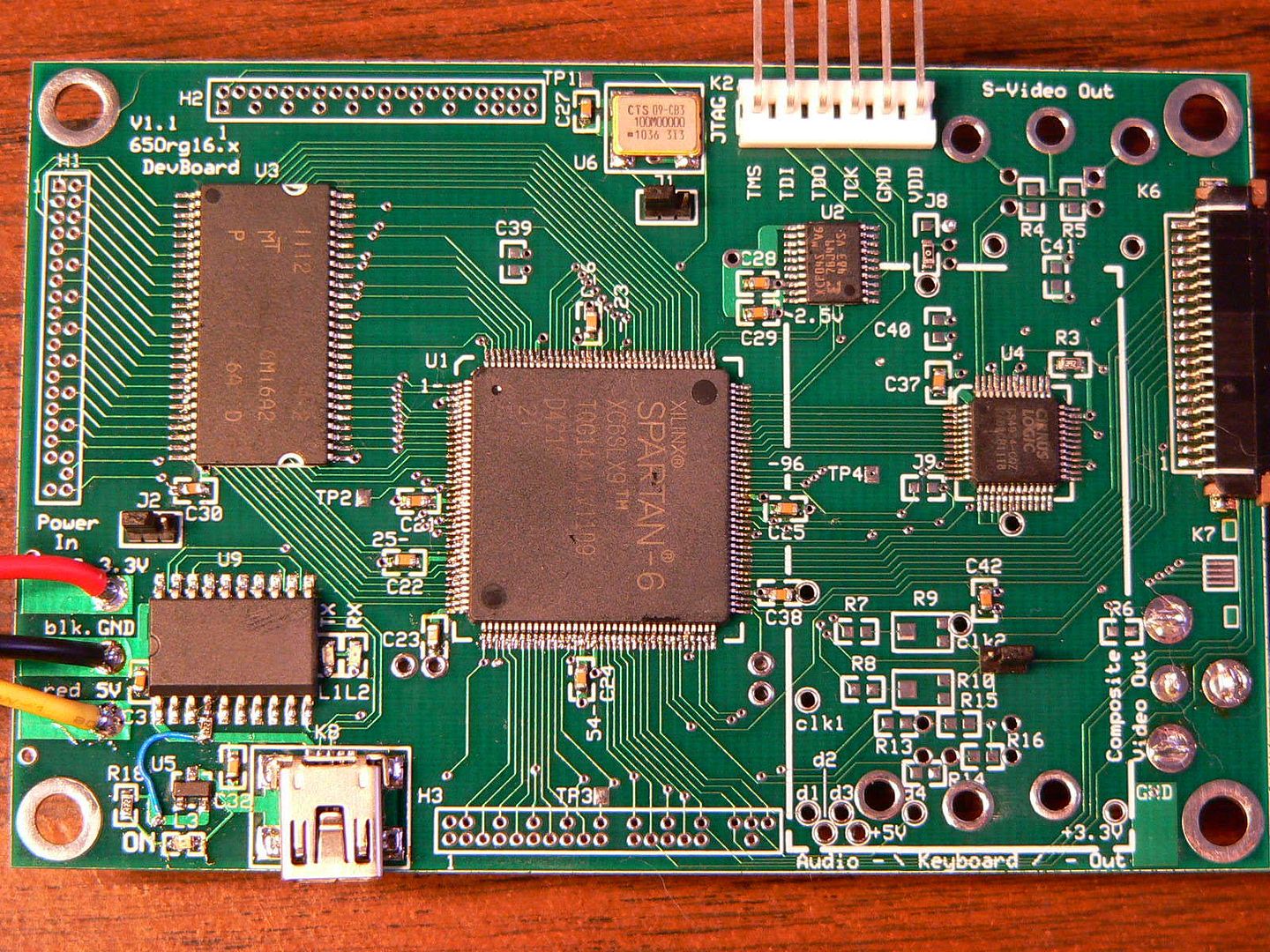
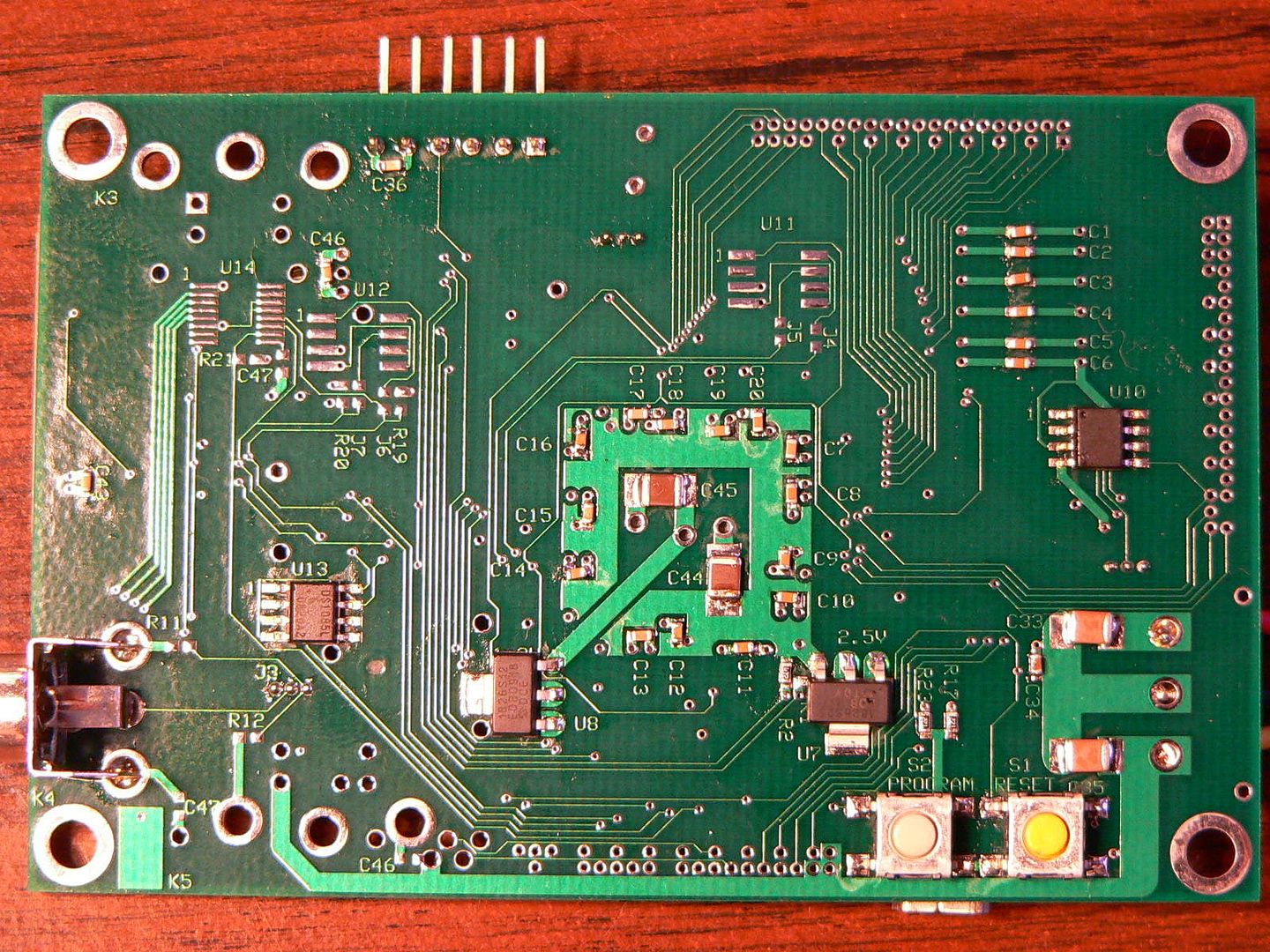
Ok, spent the free time I had over the last 2 weeks putting together a board for Arlet and this morning I have finished!!! I applied power and iMPACT saw the FPGA PROM and the Spartan 6. I programmed it with my current progress and the TFT cleared screen and C'mon's dash prompt appeared. Success! Tomorrow I can mail it off. And so now I go back to concentrate on getting the I2C core to work...
Here's some close-ups of the soldering which you can see isn't at all perfect, but it works!
TOP
BOTTOM
Posted: Tue Feb 07, 2012 4:57 pm
by Arlet
Did you use a yellow wire for 5V on purpose ? On the PCB it is marked "red"..
Posted: Tue Feb 07, 2012 5:40 pm
by ElEctric_EyE
For the old ATX12V 400W power supply I am using, I had labelled the colors according to the voltages, but the 4-wire
female connector I spliced in on the power side (meant for HDD's/CD drives) doesn't have 3.3V (orange). I haphazardly matched the wires from the power supply to what was needed on the board. In the end pay attention to the DC Voltages spec'd on the board itself, not the colors. And thanks for pointing that out! I am making many notes for V1.2...
Posted: Wed Feb 08, 2012 1:39 pm
by ElEctric_EyE
I've checked and re-checked, and I found I had left out R19&R20, the 4.7K pull-up resistors for I2C. The board has now passed "my QC"

Arlet, one final note: I guess they are the impedance matching? resistors on the video outputs. The datasheet says to either use 75 ohms or 300ohms. If you are not sure either, I will include 3 of each resistor value, 1 for composite (R6) and 2 for S-Video (R4,R5). And speaking of S-Video, if you do get around to soldering that connector (Digi-Key #CP-2240-ND), it goes on the bottom with the composite RCA connector.
Posted: Wed Feb 08, 2012 6:17 pm
by Arlet
I've checked and re-checked, and I found I had left out R19&R20, the 4.7K pull-up resistors for I2C. The board has now passed "my QC"
Arlet, one final note: I guess they are the impedance matching? resistors on the video outputs. The datasheet says to either use 75 ohms or 300ohms. If you are not sure either, I will include 3 of each resistor value, 1 for composite (R6) and 2 for S-Video (R4,R5). And speaking of S-Video, if you do get around to soldering that connector (Digi-Key #CP-2240-ND), it goes on the bottom with the composite RCA connector.
I haven't looked into the impedance before, but if you have the resistors, it sounds like a good plan to include them separately, especially since they are non-standard values.