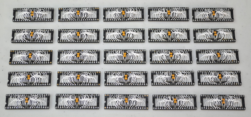
Home baked 512K 10ns SRAMs... fresh out of the oven.
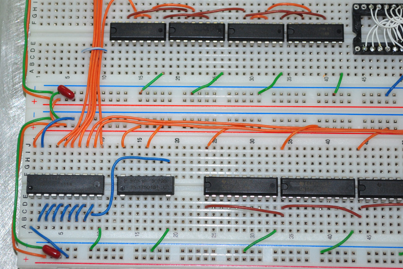
All 25 of the SRAMs will be used in this project, and there will be a smaller SRAM required for the 6502 memory.
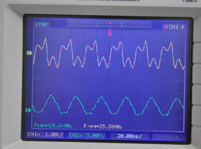
To maintain the highest image quality, I have put together a precision R2R DAC using 1% resistors.
Using the standard resistor values of R:422 and 2R:845, the resulting DC voltage is very close to the VGA standard.
Tests on my other board have shown that the 4096 color palette looks almost as good as it does shown on my PC monitor.
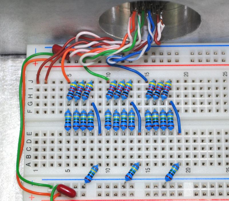
4096 Colors from a triple 4 Bit R2R DAC.
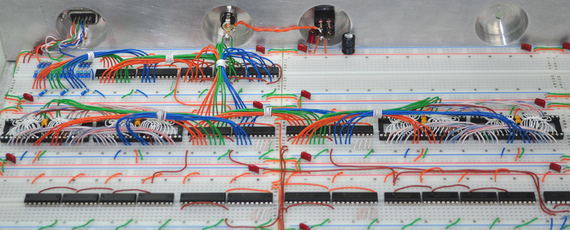
The new 4096 color 640x480 design is very different form the original 256 color 400x300 design.
Many of the ICs are the same such as the 74HC590 counters and 74HC574 registers.
Actually, besides the SRAM and AND Gates, there are no other ICs in the new design!
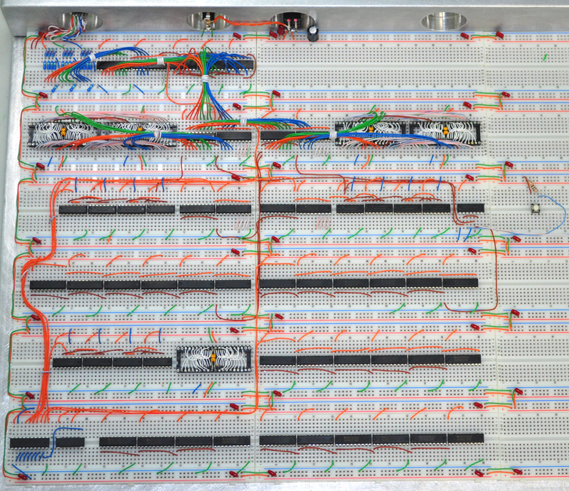
Here is my plan...
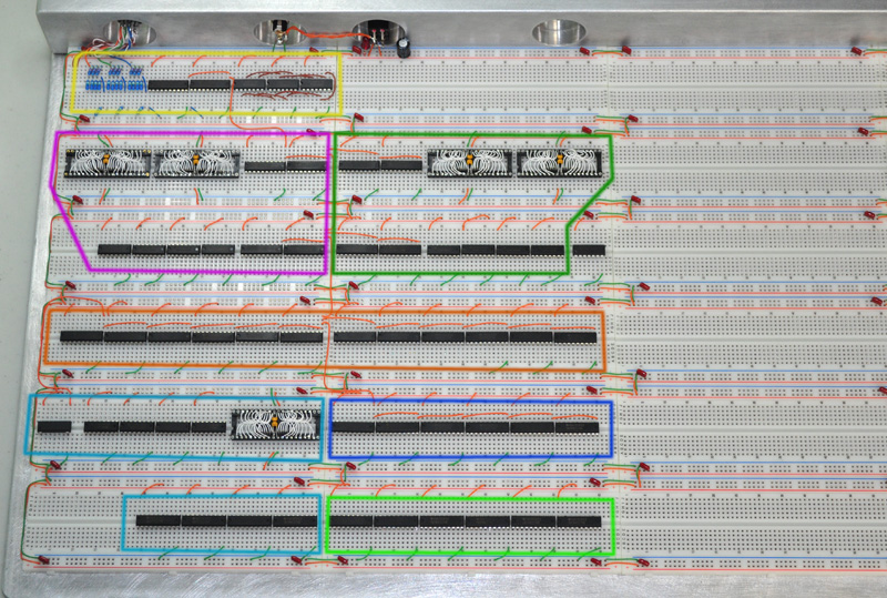
Designing the new Video Generator System.
The top Yellow box is the Blanking and Color combiner.
This circuit syncs the live pixel data and blanking periods to the rise of the pixel clock.
ICs used are 3 x 74HC08 (AND Gate) and 2 x 74HC574 (Data Register).
Below that, we have a Purple and Green set of mirror images.
These are the Dual Video Buffer SRAMs and XY Counters.
Only one is actively drawing pixels at a time while the other is available to the GPU.
ICs used are 2 x 512K 10ns SRAM, 4 x 74HC590 (8 Bit Counter) and 4 x 74HC574 (Data Register).
The lone IC is a 74HC74 Flip Flop. This is clocked to swap the Buffers and Switches.
The 6502 will call for a "Flip" just after the start of a Vertical Sync.
The orange box below the Video Buffers is the Address and Data Switcher.
This row of 12 x 74HC574 (Data Register) controls access to each of the Video Buffers.
As usual, only one side is active at any one time, sharing access to the SRAM with the XY Counters.
The light blue box to the lower left is the Sync Memory and its XY counters.
Control signals such as Horizontal Sync, Vertical Sync, and Blanking come from this memory.
This memory also sends the XY wrap and reset signals to its own counters as well as the Video counters.
This circuit consists of a 512K SRAM, 4 x 74HC590 (8 Bit Counter) and a 25MHz Oscillator Module.
The darker blue box to the right is another address and data switch for incoming GPU data.
These 6 x 74HC574 (Data Registers) sync any data coming from the Graphics Generator into the SRAM.
This switch is only on if the light green box below is not active.
The light green box below is another address and data switch for incoming CPU data.
These 6 x 74HC574 (Data Registers) sync any data coming from the 6502 into the SRAM.
This switch is only on if the dark blue box above is not active.
This data represents pixels that are directly written (or read) by the 6502 instead of the GPU.
The final light blue box is another switch to allow initial programming of the Sync Data.
These 4 x 74HC574 (Data Registers) are only active at initial power on.
The 6502 has the task of writing the Sync Memory with proper data.
Different Video Formats are possible by altering this data.
So that is my plan for now.
I fully expect it to work perfectly on the first power up.
... after all, it's just a bunch of simple gates and wires, right???
yeah, right!
More to come...
Radical Brad