6502.org Forum  Projects  Code  Documents  Tools  Forum
It is currently Sat Nov 23, 2024 5:18 am

All times are UTC


Post new topic Reply to topic  [ 842 posts ]  Go to page Previous  1 ... 37, 38, 39, 40, 41, 42, 43 ... 57  Next
Author Message
PostPosted: Wed Mar 15, 2017 10:38 pm 
Offline
User avatar

Joined: Mon May 25, 2015 2:25 pm
Posts: 690
Location: Gillies, Ontario, Canada
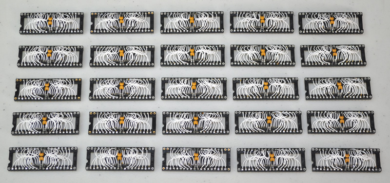
I finished soldering up the last 10 SRAMs, and have now started placing components based on my new design.

Image
Home baked 512K 10ns SRAMs... fresh out of the oven.

All 25 of the SRAMs will be used in this project, and there will be a smaller SRAM required for the 6502 memory.

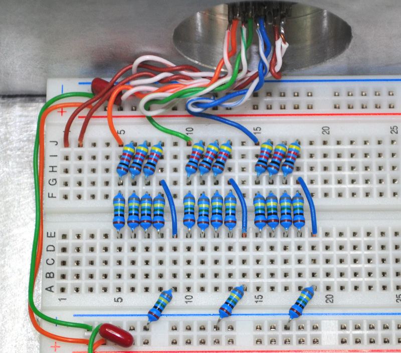
To maintain the highest image quality, I have put together a precision R2R DAC using 1% resistors.
Using the standard resistor values of R:422 and 2R:845, the resulting DC voltage is very close to the VGA standard.
Tests on my other board have shown that the 4096 color palette looks almost as good as it does shown on my PC monitor.
Image
4096 Colors from a triple 4 Bit R2R DAC.

The new 4096 color 640x480 design is very different form the original 256 color 400x300 design.
Many of the ICs are the same such as the 74HC590 counters and 74HC574 registers.
Actually, besides the SRAM and AND Gates, there are no other ICs in the new design!

Here is my plan...
Image
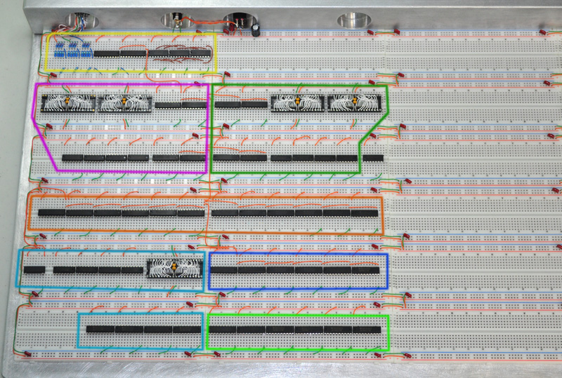
Designing the new Video Generator System.

The top Yellow box is the Blanking and Color combiner.
This circuit syncs the live pixel data and blanking periods to the rise of the pixel clock.
ICs used are 3 x 74HC08 (AND Gate) and 2 x 74HC574 (Data Register).

Below that, we have a Purple and Green set of mirror images.
These are the Dual Video Buffer SRAMs and XY Counters.
Only one is actively drawing pixels at a time while the other is available to the GPU.
ICs used are 2 x 512K 10ns SRAM, 4 x 74HC590 (8 Bit Counter) and 4 x 74HC574 (Data Register).

The lone IC is a 74HC74 Flip Flop. This is clocked to swap the Buffers and Switches.
The 6502 will call for a "Flip" just after the start of a Vertical Sync.

The orange box below the Video Buffers is the Address and Data Switcher.
This row of 12 x 74HC574 (Data Register) controls access to each of the Video Buffers.
As usual, only one side is active at any one time, sharing access to the SRAM with the XY Counters.

The light blue box to the lower left is the Sync Memory and its XY counters.
Control signals such as Horizontal Sync, Vertical Sync, and Blanking come from this memory.
This memory also sends the XY wrap and reset signals to its own counters as well as the Video counters.
This circuit consists of a 512K SRAM, 4 x 74HC590 (8 Bit Counter) and a 25MHz Oscillator Module.

The darker blue box to the right is another address and data switch for incoming GPU data.
These 6 x 74HC574 (Data Registers) sync any data coming from the Graphics Generator into the SRAM.
This switch is only on if the light green box below is not active.

The light green box below is another address and data switch for incoming CPU data.
These 6 x 74HC574 (Data Registers) sync any data coming from the 6502 into the SRAM.
This switch is only on if the dark blue box above is not active.
This data represents pixels that are directly written (or read) by the 6502 instead of the GPU.

The final light blue box is another switch to allow initial programming of the Sync Data.
These 4 x 74HC574 (Data Registers) are only active at initial power on.
The 6502 has the task of writing the Sync Memory with proper data.
Different Video Formats are possible by altering this data.

So that is my plan for now.
I fully expect it to work perfectly on the first power up.
... after all, it's just a bunch of simple gates and wires, right???
yeah, right!

More to come...
Radical Brad

Top
 Profile  
Reply with quote  
PostPosted: Thu Mar 16, 2017 5:03 pm 
Offline
User avatar

Joined: Mon May 25, 2015 2:25 pm
Posts: 690
Location: Gillies, Ontario, Canada
Since this project be moving to full 6502 control of the hardware in very short order, I have been giving my IO decode scheme some thought.

In my previous attempt, I managed to get 4MHz out of the 6502, with the bottle neck only at the read from Graphics Memory. If the 6502 only had to read and write from its own Program Memory (10ns SRAM), then I found that it would run easily at 16Mhz.

My system has no ROM, so the 6502 is directly connected to the 10ns SRAM, and I only have IO at one location from address 512-767, as mapped by a 688 comparator and some 138 decoders.

Since my IO writes are basically "set and forget", propagation is not an issue. By that, I mean that once an address (say 600) is written to, the latches take care of it from there, so the 6502 can do this at 16MHz. The reads on the other hand need to be available to the 6502 as if coming from SRAM, so propagation was the entire bottle neck.

In order to circumvent this bottleneck, I am going to try an "automatic accumulator" for IO reads. How I envision this working is like so...

1) The 6502 will set the read address in the 4Mb Graphics SRAM by setting the required 22 bits (4 bytes worth).
2) The 6502 will then send a "Read Command" to IO, by writing to that location (let's say address 600).
3) The Vulcan-74 hardware will then set the SRAM to read on the next cycle and latch in the data into the Auto Accumulator.
4) The 6502 can now do an actual read on the auto Accumulator, by reading that address (let's say 601).
5) Since the Auto Accumulator is just a 74HC574, the toggle of its OE will be as fast as 16ns.

So rather than slowing down the 6502 to 4MHz to get a direct read, it can now run at 16Mhz, doing an "ask to read" and then a read, which should still be twice as fast as going down to 4MHz. And of course, all access to Program Memory will be at the full 16Mhz.

I plan on using this Auto Accumulator idea on all IO locations to be read such as Graphics Memory, Screen Memory, Sound Memory, Joystick, Keyboard, and Cartridge ROM.

Whatever it takes to squeeze every last ounce of performance out of the 6502 without breaking my rules, which only allow common 74HC logic to be used.

As a side note, using a 10ns SRAM (preloaded with code from an external source), I was able to make a 65C02 perform perfectly stable at 20Mhz. In this test, my IO was nothing more than a single address, but it did work well.

Brad


Top
 Profile  
Reply with quote  
PostPosted: Thu Mar 16, 2017 5:12 pm 
Offline

Joined: Fri Nov 27, 2015 10:09 am
Posts: 67
Nice. Reminds me of VRAM, where you do a single read and it latches and entire row into a buffer for high speed access without contention.


Top
 Profile  
Reply with quote  
PostPosted: Thu Mar 16, 2017 5:29 pm 
Offline
User avatar

Joined: Fri Dec 11, 2009 3:50 pm
Posts: 3367
Location: Ontario, Canada
Oneironaut wrote:
Home baked 512K 10ns SRAMs... fresh out of the oven.
Yum! :mrgreen:

Quote:
The reads on the other hand need to be available to the 6502 as if coming from SRAM, so propagation was the entire bottle neck.

So, you ...
  • You tell the hardware what data you want, then you
  • come back and get that data.

Sounds workable, but is there a simpler solution that's as good, or almost? It seems to me a brief slowdown (wait state) to 4 MHz equivalent could get the job done promptly. The wait-state delay probably wouldn't be much different from the delay incurred if we had to fetch and execute an additional instruction. It might even be faster.

I know wait states have an unwelcome connotation. But I'll bet they'd be quite a lot simpler to implement -- better bang for the buck. Maybe I'm missing something. Just thinking out loud...

_________________
In 1988 my 65C02 got six new registers and 44 new full-speed instructions!
https://laughtonelectronics.com/Arcana/ ... mmary.html


Top
 Profile  
Reply with quote  
PostPosted: Thu Mar 16, 2017 7:01 pm 
Offline
User avatar

Joined: Mon May 25, 2015 2:25 pm
Posts: 690
Location: Gillies, Ontario, Canada
AN interesting idea. So basically have a FlipFLop trigger on a certain read address so that the clock is held back a cycle. For longer states, trigger a counter.

I will consider that option when I put together the IO decode circuit.

No matter what though, the 6502 is always seeing any IO or SRAM addresses "virtual", meaning that that a 22 bit address is latched before any read or write is possible. There is no memory mapped graphics in this system.

It really wouldn't matter if it took the 6502 even 10x the number of cycles to talk to the GPU, because once it sets the coordinates on a bitmap, the blitter takes over at 25Mhz bandwidth.

Brad

Dr Jefyll wrote:
Oneironaut wrote:
Home baked 512K 10ns SRAMs... fresh out of the oven.
Yum! :mrgreen:

Quote:
The reads on the other hand need to be available to the 6502 as if coming from SRAM, so propagation was the entire bottle neck.

So, you ...
  • You tell the hardware what data you want, then you
  • come back and get that data.

Sounds workable, but is there a simpler solution that's as good, or almost? It seems to me a brief slowdown (wait state) to 4 MHz equivalent could get the job done promptly. The wait-state delay probably wouldn't be much different from the delay incurred if we had to fetch and execute an additional instruction. It might even be faster.

I know wait states have an unwelcome connotation. But I'll bet they'd be quite a lot simpler to implement -- better bang for the buck. Maybe I'm missing something. Just thinking out loud...


Top
 Profile  
Reply with quote  
PostPosted: Thu Mar 16, 2017 7:41 pm 
Offline
User avatar

Joined: Fri Dec 11, 2009 3:50 pm
Posts: 3367
Location: Ontario, Canada
Oneironaut wrote:
So basically have a FlipFLop trigger on a certain read address so that the clock is held back a cycle. For longer states, trigger a counter.
Yup. Either freeze the clock or pull RDY low -- either way is pretty easy. These circuits use RDY. (And for 8 or fewer wait-states a shift register can replace a counter. Whichever works out to be simplest.)

Quote:
a 22 bit address is latched before any read or write is possible. There is no memory mapped graphics in this system.
Outputting that 22 bit address is a problem with a zillion solutions, some of them funner than others. :) On 'C02 it's remarkably easy to roll your own instructions, particularly for a simple data move (such as zero-page to a '574, or Immediate-Operand to a '574).

_________________
In 1988 my 65C02 got six new registers and 44 new full-speed instructions!
https://laughtonelectronics.com/Arcana/ ... mmary.html


Top
 Profile  
Reply with quote  
PostPosted: Sun Mar 19, 2017 12:10 am 
Offline
User avatar

Joined: Mon May 25, 2015 2:25 pm
Posts: 690
Location: Gillies, Ontario, Canada
Since I am now building this version with a somewhat tested plan, I can start from the top down.
It is always easier to route all of the clock and control lines, and then move onto data and address lines.

I wired up all of the OE and CLK lines for the 574's, and then ran the clock lines around the board.
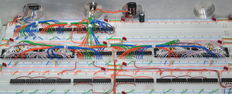
Once all of those lines were down, I started at the top, working on the 12 Bit Dual Video Data Bus.
I decided to use Red, Green, and Blue lines to show the actual colors for each of the 3 x 4 bit Data Lines.

Image
Routing the Dual Buffer 12 Bit Data Lines.

The photo above shows how the Dual Buffers (512K x 2) feed their respective 574's, and then into the switch.
The switch is a set of two 574's that then feed 12 AND gates that sync the blanking with the pixel data.
The AND gates then feed another set of 574's to re-sync the pixel data to the main system clock.

I also tested the routing of the clock by viewing the waveform on my scope, but there were issues.
In this version of the Video Generator, the clock has to drive 34 chips directly!
But it seems that the single oscillator module did not have the gusto to push that many ICs.
The waveform was so weak and rounded off that it looked like a 2 volt pure sine-wave on my scope.
There were losses in the other design, but this time the drive capacity is a real problem.

I thought about adding gates at each "intersection"m but this would skew the clock be a few nanoseconds.
Instead, I drove the clock into a 74HC245, and tied all of the inputs together.
This would allow 8 individual and fully synchronous clock drivers to be available to the board.
I then divided the clock segments up equally (and mostly in rows), routing a line for each...

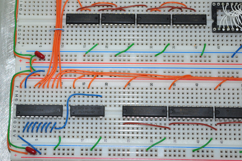
Image
The 74HC245 drive out seven synchronous clock lines.

You can see the 25.175MHz clock module driving all 8 inputs on the 74HC574 buffer.
I used 7 of the 8 possible outputs, and now each output line only has to drive 5 or 6 ICs.

I am no sure if this is a perfect solution, as I did not find any examples in my searches of this being used.
But once wired and tested, the resulting waveform at each row was as clean as the original clock source...

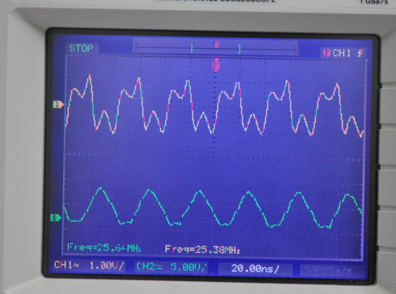
Image
The master clock at the bottom, and furthest clock at the top.

The waveform shown above is not pretty, but that's only because of the way I have my scope tapped into the board.
The top waveform is as good as the unloaded clock module at each "intersection", so I think this is going to work perfectly.

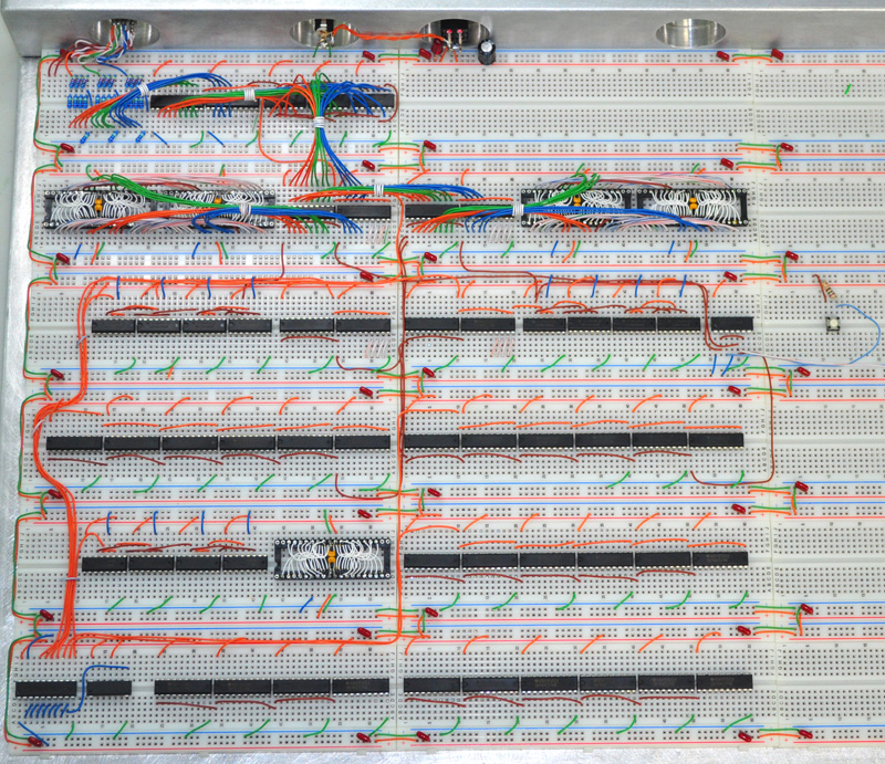
Here is the board as of tonight. I used Red wires to route the clock lines from the "distribution chip"...

Image
There are now seven individual clock lines being routed.

I also connected the 6 sets of cascaded 74HC590 counters (12 counters in total), and tested the signal.
As expected, all of the counters were getting a nice clean clock signal, and counting perfectly.

It's interesting to note that the new Video Generator now takes up exactly twice as much space as the original.
The original 400 x 300 x 256 System fit on one column, and the new 640 x 480 x 4096 System takes two columns.
Not a bad deal, since the number of bits per second has increased dramatically...

Version One = 57,600,000 Bits Per Second Bandwidth
Version Two = 221,184,000 Bits Per Second Bandwidth

Yes, that number is correct!
This mess of 1980's logic chips pushes out 221 Million Bits Per Second to make a Video Frame!

On my next free session, I will connect the counters from one side to the SRAM, and see if I get video.
Actually, there is a bit more to it than that. To see random pixels in this design, I have to...

- Connect at least one set of X/Y counters to one of the SRAM Video Memories.
- Connect the Sync Memory to its dedicated X/Y counter system.
- Connect the Sync Memory Address and Data Switch to the Sync Memory.
- Connect a micro-controller to the Sync Switch in order to program the Video Mode Data.

From there, I can then connect the second Video Buffer, and then the A/B switching logic.
It will take a few more free days to actually see some images on the screen, but that's not too bad.
Once the Video System is operational, I can then start prototyping the new hi-speed Graphics System.

I don't call it a Sprite Generator anymore because I am mixing the Playfield Generator and Sprite Generator together.
The new Graphics System is uncharted territory for me, and development is coming directly from coffee stained notebooks!

This is where the real fun shall begin again.

Later!
Radical Brad


Top
 Profile  
Reply with quote  
PostPosted: Sun Mar 19, 2017 2:47 am 
Offline
User avatar

Joined: Fri Dec 11, 2009 3:50 pm
Posts: 3367
Location: Ontario, Canada
Oneironaut wrote:
Since I am now building this version with a somewhat tested plan, I can start from the top down.
It is always easier to route all of the clock and control lines, and then move onto data and address lines.
Lookin' good, Brad. :) Nice that you're able to expedite the routing.

Oneironaut wrote:
The switch is a set of two 574's that then feed 12 AND gates that sync the blanking with the pixel data.
The AND gates then feed another set of 574's to re-sync the pixel data to the main system clock.
Right. If you didn't re-sync the pixel data then blanking could cause the leftmost and rightmost pixel of each scan line to have an irregular appearance compared to all the other pixels in the line.

But, unless I'm missing something, the same job can be done using fewer IC's. Let me know if I've got these details right. Presently you're using...
  • three 14-pin chips (to get 12 AND gates, for the blanking aka Clear function)
  • two 20-pin chips (to get a 12-bit register)

Instead what I propose is...
  • three 16-pin chips, each of them a 4-bit register with synchronous clear. Together they form a 12-bit register.


What's that you say? You didn't know the 74xx "vocabulary" includes a 4-bit register with synchronous clear? :P :P :P

I have to razz you about this because I'm referring to the 74xx163 counter -- a chip that's a favorite of mine, but one regarding which you made some unflattering comments in a couple of posts last year. And now it comes to your rescue. (Well, maybe not now, as it's probably too late to backtrack. But in your next 74xx video project you can use it.)

The '163 is able to Hold, Count, Load or Clear. The lowest-priority mode is Hold, but that's overridden by Count which in turn is overridden by Load which in turn is overridden by Clear. All changes are synchronous to the rising edge of the clock input.

In the Vulcan video application the '163 Load enable inputs would be hard-wired to the active state and the count-enable inputs would be don't-care. The Clear enable inputs would accept the video blanking signal (same as what presently feeds those AND gates), resulting in either a synchronous Load or a synchronous Clear with every clock. (When serving merely as a register the counter isn't required to count.)

I love this project, but I hope you'll agree that worthwhile applications exist for the ever-versatile '163!

-- Jeff

_________________
In 1988 my 65C02 got six new registers and 44 new full-speed instructions!
https://laughtonelectronics.com/Arcana/ ... mmary.html


Last edited by Dr Jefyll on Sun Mar 19, 2017 2:43 pm, edited 1 time in total.

Top
 Profile  
Reply with quote  
PostPosted: Sun Mar 19, 2017 6:20 am 
Offline
User avatar

Joined: Thu May 28, 2009 9:46 pm
Posts: 8507
Location: Midwestern USA
Oneironaut wrote:
Instead, I drove the clock into a 74HC245, and tied all of the inputs together...You can see the 25.175MHz clock module driving all 8 inputs on the 74HC574 buffer...The waveform shown above is not pretty, but that's only because of the way I have my scope tapped into the board.

This might be a good place to substitute a 74AC245, with its 24 mA output capability. Or, perhaps use an oscillator with twice the desired frequency and run it through a 74AC74 flop.

_________________
x86?  We ain't got no x86.  We don't NEED no stinking x86!


Top
 Profile  
Reply with quote  
PostPosted: Sun Mar 19, 2017 6:47 am 
Offline
User avatar

Joined: Fri Aug 30, 2002 1:09 am
Posts: 8544
Location: Southern California
BigDumbDinosaur wrote:
This might be a good place to substitute a 74AC245, with its 24 mA output capability. Or, perhaps use an oscillator with twice the desired frequency and run it through a 74AC74 flop.

Hmmm... The 74AC's faster edge rate might get pretty interesting on a solderless breadboard with long connections and no ground plane.

_________________
http://WilsonMinesCo.com/ lots of 6502 resources
The "second front page" is http://wilsonminesco.com/links.html .
What's an additional VIA among friends, anyhow?


Top
 Profile  
Reply with quote  
PostPosted: Sun Mar 19, 2017 2:33 pm 
Offline
User avatar

Joined: Mon May 25, 2015 2:25 pm
Posts: 690
Location: Gillies, Ontario, Canada
Thanks for the comments and ideas.

Jeff, I do member you suggestion to use the 163 output version from this post...

viewtopic.php?f=4&t=3329&start=45#p38632

I did try that method last year, and found that there was a very slight variance between the counters.
It was perhaps only half a nanosecond (or less), but was enough to make the phase adjustment difficult.
I had to resync with another 574 after the 163 chain, which put the chip count back to the same.

This year, I am switching / syncing 15 bits... 4 Red, 4 green, 4 Blue, Hsync, Vsync, and Blanking.
So even using the 163, I would still require a downstream 574, so it would be a one chip (less) gain.
With the video frame running at 640 rather than 400 now, I also bet the phase error would be more noticeable.

But, on the flip side, I do actually intend to become friends with the 74HC163 very soon.
My new Graphics Generator design is to be fully synchronous, and will require 12 synced 74HC163 counters in total.
To get (hopefully) at least 10MHz of bandwidth this time, I intend to do a 3 stage pipeline.
This is how the Video Generator currently works, and the 74HC590 are also synchronous in operation.

The "glitch" I found in the 163 is that you have to clock in the reset (hold it during the clock transition).
Unlike the 590, which is happy to see any pulse on reset, and then spit out a zero whenever the next clock happens.
To beat this goofy requirement, I am going to use a flip flop to send the reset signal, and qualify it with the bi-phase clock.
... yeah, ideas copied from my buddy the 6502!

When I drop down the dozen 163 counters, I will tell them that they come highly recommended by Dr Jefyll.
Maybe they will play nice for me then!


Garth and Dino,

I have made it one of my rules to only use HC logic, but I may allow one instance of AC if it really ups performance.
And only if I cannot do the same with pure chip count alone.
If I can gain one nanosecond by adding 50 HC chips, I will do that before I add one AC chip.

You are also correct on the noise factor. I am bracing for the noise that the 65C02 is going to add as well.
Seems, it has that high switching rate as well, and in another project it spewed noise all over an otherwise nice design.
I do have some crazy ideas on how to beat the noise out of my 6502 though, and when the time comes will try them all.

I will also admit to having purchased a few 74AC138s just in case i need them to get the 6502 speed up later.
Having tested the 6502 at 20MHz (and 25 MHz), using a direct to SRAM (10ns) setup, I now it can indeed perform.
In my last Vulcan-74 version, I only managed to get 4MHz out of the 6502. It did 8MHz if it only had to write to IO.

My new plan is to also pipeline the 6502 through levels of 574s.
Since it can never issue consecutive reads or writes (on every true cycle), it's ok if the command is "in the pipe" for a few cycles.
This isolation will also allow it to live far away on the board, and perhaps on an isolated power supply.
The 574 will "shuttle" the data into the core of the IC city, and this may actually cancel the noise problem as well.

So many new ideas to try here!
I definitely appreciate the comments and ideas from everyone here.
Being just a 6502 "hacker" amongst the real experts here, I know the answers shall be found!
I am still getting pummeled by this crazy flu, so I have the day down here to run some counter lines.

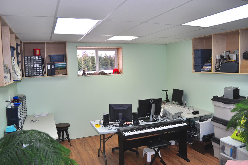
It's always interesting to see where people do their hacking and building. Here is my "Lab"...

Image

The room in my basement is a work in progress, but I did get the drop ceiling and basic cupboards in last year.
I still have to build proper desks, and cupboard doors, and trim, but it's getting there.
Vulcan-74 currently takes up a full 6 foot desk, but that's to be expected with a 48 breadboards wired together!

Cheers!
Brad


Top
 Profile  
Reply with quote  
PostPosted: Sun Mar 19, 2017 2:56 pm 
Offline
User avatar

Joined: Thu May 28, 2009 9:46 pm
Posts: 8507
Location: Midwestern USA
GARTHWILSON wrote:
BigDumbDinosaur wrote:
This might be a good place to substitute a 74AC245, with its 24 mA output capability. Or, perhaps use an oscillator with twice the desired frequency and run it through a 74AC74 flop.

Hmmm... The 74AC's faster edge rate might get pretty interesting on a solderless breadboard with long connections and no ground plane.

No doubt!

_________________
x86?  We ain't got no x86.  We don't NEED no stinking x86!


Top
 Profile  
Reply with quote  
PostPosted: Sun Mar 19, 2017 3:23 pm 
Offline
User avatar

Joined: Mon May 25, 2015 2:25 pm
Posts: 690
Location: Gillies, Ontario, Canada
BigDumbDinosaur wrote:
GARTHWILSON wrote:
BigDumbDinosaur wrote:
This might be a good place to substitute a 74AC245, with its 24 mA output capability. Or, perhaps use an oscillator with twice the desired frequency and run it through a 74AC74 flop.

Hmmm... The 74AC's faster edge rate might get pretty interesting on a solderless breadboard with long connections and no ground plane.

No doubt!


All breadboards are fastened to a 1/4 thick aluminum plate that is connected to ground.
Would that not count as a fairly substantial ground plane?

Brad


Top
 Profile  
Reply with quote  
PostPosted: Sun Mar 19, 2017 3:34 pm 
Offline
User avatar

Joined: Fri Aug 30, 2002 1:09 am
Posts: 8544
Location: Southern California
Oneironaut wrote:
All breadboards are fastened to a 1/4 thick aluminum plate that is connected to ground.
Would that not count as a fairly substantial ground plane?

Not at all. I need to find a good explanation of how a ground plane works at the frequencies of interest here, but I don't have the time at the moment. It's not hard to understand, just hard to explain.

_________________
http://WilsonMinesCo.com/ lots of 6502 resources
The "second front page" is http://wilsonminesco.com/links.html .
What's an additional VIA among friends, anyhow?


Top
 Profile  
Reply with quote  
PostPosted: Sun Mar 19, 2017 3:39 pm 
Offline
User avatar

Joined: Tue Nov 16, 2010 8:00 am
Posts: 2353
Location: Gouda, The Netherlands
The key is to visualize currents as going in a loop, with the signal going from A to B, and the return current through ground back from B to A. For best integrity, you want the return path to be as close as possible to the signal path.

Whether an external plate is useful depends on how close it is to the signal, and how much of a detour the current has to take to get on the plate, and back off.


Top
 Profile  
Reply with quote  
Display posts from previous:  Sort by  
Post new topic Reply to topic  [ 842 posts ]  Go to page Previous  1 ... 37, 38, 39, 40, 41, 42, 43 ... 57  Next

All times are UTC


Who is online

Users browsing this forum: Google [Bot] and 32 guests


You cannot post new topics in this forum
You cannot reply to topics in this forum
You cannot edit your posts in this forum
You cannot delete your posts in this forum
You cannot post attachments in this forum

Search for:
Jump to: