Posted: Wed Oct 20, 2010 6:21 pm
OK, so when I said the bidirectional bus was working inside the FPGA, it was/IS working for the single 7-bit port that controls the upper banked addresses A14-A20, to the 2Mx8 RAM. The software is successfully performing INC on the SRAM Bank Register... I had intentions of using a building block approach to make more ports since this one worked...
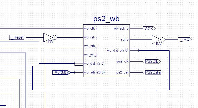
But when I needed another port to read from the 'PS2 core' keyboard interface I put in the FPGA, everything went to crap. Got tons of errors. Bidirectional errors. Even though the PS2 core synthesized perfectly and I easily made a symbol...
So I went back to the basics this morning, and came up with this: viewtopic.php?t=1665 , after Andre's post.
I may just relax awhile and try to learn a little more about FPGA's while at the same time working out some more software routines for the display since everything is working so nicely as far as the display & banked RAM is concerned. But, I am at a crossroads. I'm pretty sure I could get the internal registers I need to work if I rewire in the CPLD I have in mind, a 100-pin QFP Coolrunner II XPLA3. But then the PS2 core wouldn't fit into it. I know it will fit into the XC2S15, even though all by itself, the PS2 core uses 50% of the FPGA resources. But if I don't have the PS2 interface I am stuck reprogramming the EEPROM after every simple modification.
......
I've noticed on most if not all FPGA development boards, they have a CPLD onboard to go hand in hand with the FPGA. I'm starting to think that's what I may need here as well. Put all the cores (PS2, IDE, USB, I2C) into 1 FPGA with separate Input data buses and Output data buses, and then bring them all together at the CPLD to interface to the 6502 and memory.
Once again, starting from scratch! But I may just relax awhile and experiment with what I've got...