You can get RAM, ROM, and plenty of 65xx I/O in your 6502 sytem using a single quad 2-input NAND gate 14-pin IC. Here's one way to do it:
Use one NAND to invert A15, the high address bit, to get A15\. Connect A15\ to the CS\ and OE\ of a 27c256 32Kx8 EPROM, giving you ROM from 8000 to FFFF.
Connect A14 to a 62256 32Kx8 SRAM's A14 and OE\ inputs, and use another NAND for the RAM's CS\ input such that
CS\ = NOT(phase_2 AND A15\). This way you use half the 32Kx8 RAM (16KB), from 0000 to 3FFF.
Connect a third NAND's inputs to A14 and A15\ (derived above), and its output to the CS\ inputs of up to ten I/O ICs like the 6522 and 6551 in the 4000-7FFF range. Individual CS inputs of the various ICs can then go to individual address lines A4,A5,...A13. (The 6522's need A0 to A3 for register selects.)
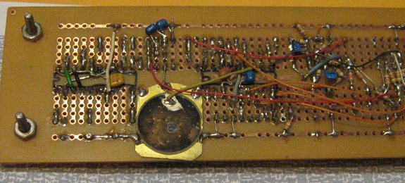
This scheme is more-or-less what I have on my workbench computer with 3 65c22's and 3 65c51's. Four more could be accomodated without any more glue logic. A tradeoff for the simplicity is that some address ranges in the 16K I/O area duplicate others and thus are essentially unusable; but it fits the purpose nicely.
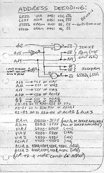
For more simple address-decoding schemes, see the address-decode section of my 6502 primer. (Actually, you will find the above to be more clear there too.) There is also a basic 6502 computer schematic showing the simple address decoding at http://wilsonminesco.com/6502primer/pot ... ml#BAS_CPU .