Page 14 of 15
Re: Breaking 6502 apart
Posted: Thu Jul 04, 2013 6:15 pm
by enso
I updated my PLA utility...
Is org's PLA utility (from Jul 2012) still around? The url does not work...
Re: Breaking 6502 apart
Posted: Sun Jul 07, 2013 3:22 pm
by org
Re: Breaking 6502 apart
Posted: Fri Aug 09, 2013 7:12 am
by org
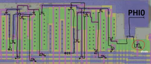
Hello everyone, long time no see )
Please help me to analyse this circuit :
And logic representation :
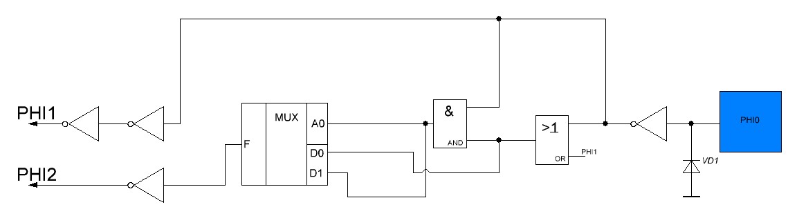
The problem is following: as you know, PHI1/PHI2 is lag a little over input PHI0. But 6502 documentation says PHI1/PHI2 also have a slighty extended low period, to ensure that PHI1 and PHI2 are never high at the same time.
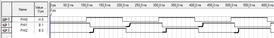
Can someone simulate this circuit and check for PHI1/PHI2 timing diagram ?
It should be someting like that :
Re: Breaking 6502 apart
Posted: Fri Aug 09, 2013 1:24 pm
by BigEd
Hi Org
please check against this circuit, which looks more plausible:
viewtopic.php?f=1&t=2412#p24074
I followed the instructions at
viewtopic.php?p=13550#p13550 and was able to capture these images of a simulation of the 6502 netlist (as found in Peter Monta's github project):
The nodenames & numbers are from the visual6502 netlist.
Cheers
Ed
Re: Breaking 6502 apart
Posted: Mon Aug 12, 2013 11:16 am
by org
My friend, more enlightened in the hardware stuff said it is "asymmetric cascade inverter", which delays the rising edge, so it seems that the lower level of PHI1/PHI2 is longer than the upper.
This mean Balazs clock envelopes are slighty incorrect.
Re: Breaking 6502 apart
Posted: Wed Aug 14, 2013 7:00 am
by org
Removed all circuits from circuitlab. Dont like it greedy politics.
Now converting all circuits into sPlan format and doing double check.
Latest circuitlab circuits can be found here (may be outdated in near future) :
http://breaknes.com/files/6502/6502_circuitlab.zip (2 MB)
Also I want to introduce project wiki :
http://wiki.breaknes.com (currently only on russian)
Re: Breaking 6502 apart
Posted: Sat Aug 17, 2013 7:08 pm
by org
Revised approach to the device debugger. Now its made in the form of a scalable circuit image layout with controls located on top of it and also scaled along with a picture.
Simulated module passing list of "triggers" to the core, which can be controlled through debug interface.
Going to make it as tabbed interface for different parts, when I get rid with Qt

Execution simply made by pressing "Next Step" button, which execute "Step" procedure of simulated ciruit and toggles input clock.
Re: Breaking 6502 apart
Posted: Wed Sep 25, 2013 9:13 am
by org
Hi
I put my latest circuits here
Re: Breaking 6502 apart
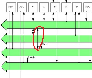
Posted: Wed Sep 25, 2013 6:22 pm
by BigEd
Hanson's diagram shows SB also connecting to ADH through pass gates...
Re: Breaking 6502 apart
Posted: Thu Sep 26, 2013 5:03 am
by org
It exist :
Re: Breaking 6502 apart
Posted: Thu Sep 26, 2013 6:43 pm
by BigEd
Oh! I didn't see it...
Re: Breaking 6502 apart
Posted: Fri Sep 27, 2013 10:38 am
by org
Nice decoder circuit.
Re: Breaking 6502 apart
Posted: Sun Oct 26, 2014 7:10 pm
by org
Complete 6502 interrupt processing circuit.
And short description.
Input pads /NMI, /IRQ, /RES are saved in input triggers.
Interrupt generation circuit additionally requires 6 and 7 cycles (since they do not arrive from decoder) (control signals BRK6E and BRK7). Control signal BRK6E begins during the PHI2 of 6th cycle and ends during PHI1 of 7th cycle (overlap 6 and 7 cycle). This is done in order to determine the edge of the signal /NMI. Edge detection of /NMI based on classic edge detect circuit (two cross-coupled RS-triggers).
The signal /RES is further saved on the RESET FLIP/FLOP, as it is required for other random logic circuits (in particular for a special control of R/W pad during reset).
The fact of the arrival of any interrupt reflected on B-flag, the output of which (B_OUT) forces the processor to execute BRK instruction (opcode 0x00). Thus developers unified processing of all interrupts.
Last small circuit generates an interrupt address (or vector) (control lines 0/ADL0, 0/ADL1 and 0/ADL2), which is reflected on 3 bits of the address bus.
The interesting thing is affection of BR2 (Branch T2) and T0 (Execute Cycle 0) control lines on interrupt detection (IRQ CHECK).
In case you wish to play with it in
Logisim, you can grab it from SVN:
https://code.google.com/p/breaks/source ... 2/INT.circ
PS. All D-latches are level-triggered. Those one with invertor are PHI1 driven (and in turn PHI2 driven without it).
Re: Breaking 6502 apart
Posted: Mon Nov 03, 2014 12:24 am
by org
Random logic + Dispatcher.
Everything seems to work fine

Next step : connect all things together, try to execute some instruction and examine controls to bottom part.
Re: Breaking 6502 apart
Posted: Sat Nov 08, 2014 1:50 pm
by org
Here we go !
Complete top part 6502 simulation in discrete logic elements!
https://code.google.com/p/breaks/source ... ANDOM.circ
Enjoy
Sadly its impossible to simulate full 6502 in Logisim, since it doesn't support bidirectional wires and I have no clue how to implement bus-to-bus connections there.
I'm going to implement it in Verilog, check on CPLD and rewrite on C, for my emulator project.
PS. I fixed some bugs in random logic, check updated version in attach.