Page 13 of 15
Posted: Thu Apr 14, 2011 5:13 am
by Arlet
To get into the microcode, means adding an extra 'if( RDY )' before the case statement, like so:
Code: Select all
/*
 * Microcode state machine
 */
always @(posedge clk or posedge reset)
    if( reset )
        state <= BRK0;
    else if( RDY) case( state )
        DECODE  :
            casex ( IR )
                8'b0000_0000:   state <= BRK0;
It doesn't look like RDY support is all that complicated, but it requires some care if you want to do it with minimum of extra code/resources.
Posted: Thu Apr 14, 2011 6:56 pm
by ElEctric_EyE
I tried inserting that bit of code, also declaring RDY in the cpu module. Ran a quick sim with the RDY pin grounded, and after a quick pulse to reset, it does indeed hold the state of the cpu. With the RDY pin high it runs normal.
Seems easy, but you must really know what you're doing with Verilog Arlet, if you can make a change like that with such a small amount of code!
I'll try it out in the hardware soon...
Posted: Thu Apr 14, 2011 7:27 pm
by Arlet
Well, some more checks for RDY need to be added, otherwise things will go wrong with some instructions.
For instance, if you try holding RDY low while in RTI2 state, I think you'll see the AB value change every cycle, when it's supposed to be holding still.
As a minimum, I think you'll also need these changes:
Code: Select all
always @(posedge clk)
    if( RDY ) begin
        ABL <= AB[7:0];
        ABH <= AB[15:8];
    end
And in ALU.v:
Code: Select all
always @(posedge clk)
        if( RDY) begin
            OUT <= temp[7:0];
            CO  <= temp[8] | CO9;
            Z   <= ~|temp[7:0];
            N   <= temp[7];
            V   <= AI[7] ^ BI[7] ^ temp[7] ^ temp[8];
            HC  <= temp_HC;
        end
The ALU module needs to be extended with a 'RDY' input.
I haven't tested any of this, so I'm not 100% confident this is correct.
Posted: Thu Apr 14, 2011 9:29 pm
by ElEctric_EyE
...I haven't tested any of this, so I'm not 100% confident this is correct.
Consider me a beta tester then!
Granted, the software/hardware I am using now is not very taxing and doesn't test alot of different situations, but as I progress, the assembly will present more of a load and will put your alu/cpu modules through some tasks.
I'm planning to port over the 65C02 software I made for the PWA project where I was shifting and testing multiple sized character data and plotting the pixels on the 640x480 hi-res display. A little bit of math there...
I had already made a
video of what the 3rd stage of the PWA project does @20MHz, and that was with discrete components. It consisted of a WDC65C02, 10ns 2Mx8 SRAM, 200ns 512Kx8 EEPROM, and a Spartan2 for a PS2 core and address decoding/RAM/EEPROM banking. It also used my "on the fly" O2 clock synchronizer to slow down the CPU and copy data from the EEPROM to RAM without program interruption. Looking back, it's too bad the Spartan 2 family doesn't have resources for internal RAM/ROM, or I'd still be experimenting with them...
I think it's time to do a comparison with the 6502SoC @38MHz and the 3rd stage PWA for my own "awe" factor, and for testing Arlet's 6502 core just to get the 6502SoC up to speed for further testing....
Posted: Fri Apr 15, 2011 11:56 am
by Arlet
This weekend, I'll probably have some time to play with the RDY changes myself.
I just started looking at it, and the changes I mentioned above are certainly not enough. First of all, the IR value gets messed up as soon as RDY is asserted in the DECODE state.
OK. This looks like it may work:
http://ladybug.xs4all.nl/arlet/fpga/650 ... 502rdy.zip
I needed an extra MUX in the (already long) DI path, so I expect some impact on the timing.
Posted: Mon Apr 18, 2011 1:44 am
by ElEctric_EyE
Tonight after coming home from work, I was looking over previous posts and manually entering Arlet's (3) previous RDY mod's to be updated in the CPU.v / ALU.v modules in my new schematic. That is, before I realized his edit!
I would like to ask a Verilog beginners question at the very bottom...
Excellent! I will be able to test the RDY in the hardware once I get the Flash successfully programmed. I'm currently working out a few issues now with system running @12MHz to accommodate the slow 70ns access time of the Flash. I'm trying to implement a top level bi-directional bus that goes to the Flash because I need to program it for a Chip Erase. Before, I was just trying to read from the Flash, but now I need to send 6 consecutive data at certain addresses for the Chip Erase. Got the software figured out, but...
Once I get it working, I'll be able to test RDY when the system is running @38MHz, and I plan to use a DCM, not just FF's. Will put wait states on everything accessed off chip, i.e. display, Flash, etc. Internal RAM and ROM will run full speed at all times.
As I mentioned before somewhere, I have my eye on the Spartan 6 and the same bi-directional bus structures apply to it. Although it seems to have different OBUF's, ISE auto-updates the design. Why Spartan 6? Because, I can solder it (a 144-pin QFP package) and when I put the current design on the Spartan 6, max speed (according to ISE) went from 51MHz to 89MHz...
My Verilog Newbie Question:
Are multiple "always" statements that are present inside of a module handled instantaneously, or is there a priority or a delay when instantiated? I ask this because I noticed you put RDY assignment last in the cpu module, while I had put it after reset. Was wondering if this minute detail affects anything?
Posted: Mon Apr 18, 2011 5:22 am
by Arlet
Are multiple "always" statements that are present inside of a module handled instantaneously, or is there a priority or a delay when instantiated? I ask this because I noticed you put RDY assignment last in the cpu module, while I had put it after reset. Was wondering if this minute detail affects anything?
All the "always" blocks are done simultaneously. So, if you have something like this:
Code: Select all
reg RDY1 = 1;

always @(posedge clk )
    RDY1 <= RDY;
It gets implemented as a D-flipflop, clocked by 'clk', and with RDY as D-input, and RDY1 as the Q-output. It doesn't matter where this block is in the module.
On the other hand, when you have something like this:
Code: Select all
always @(posedge clk )
    if( reset )
        IRHOLD_valid <= 0;
    else if( RDY ) begin
the 'reset' has a higher priority than 'RDY'.
Posted: Tue Apr 19, 2011 4:15 pm
by ElEctric_EyE
Thanks for the explanation...
I'm noticing a problem I'm having using the JSR.
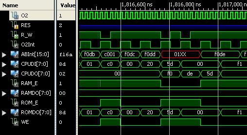
Looking at ISim when a JSR $F0DE occurs, I see $20 on the 6502 DI, indicating the JSR. Then I see the $FO then $DE on the 6502 DO during the next 2 cycles. During this time on the 6502 address bus I see $01XX, and the internal RAM is active getting this bad address. Not sure how to proceed...
Posted: Tue Apr 19, 2011 4:51 pm
by Arlet
It looks like those 2 cycles are pushing the return address (F0, DE) on the stack, and that you forgot to initialize the stack pointer.
Try adding 'statename' to the waveform, and the 'S' register.
This is what I get (without RDY), using this code:
Image no longer available: http://ladybug.xs4all.nl/arlet/jsr.png
These are the states:
JSR0: push MSB return address on stack, fetch LSB destination (D1 on DI)
JSR1: push LSB return address on stack
JSR2: write stack pointer back to S register
JSR3: fetch MSB destination (F7 on DI)
Posted: Tue Apr 19, 2011 4:58 pm
by ElEctric_EyE
...you forgot to initialize the stack pointer....
How do I go about that?
Posted: Tue Apr 19, 2011 4:59 pm
by Arlet
Like you do on a real 6502:
Posted: Tue Apr 19, 2011 5:18 pm
by ElEctric_EyE
I don't ever remember having to do this on the Commodore 64, but it used a 6510. Maybe there's a difference there? Maybe you just helped me fill in a long time knowledge gap... Either way, it works. Thanks again!
So, the $FF tells the 6502 that the stack will be $0100-$01FF?
Posted: Tue Apr 19, 2011 5:27 pm
by Arlet
No, the stack is always $0100-$01FF, but if you don't set the stack pointer, it will be initialized as a random value. On a real 6502, it may be initialized as $75 for instance. If you then do JSR, it will push the return address on $0175 and $0174. As the stack pointer reaches $00, and you push, it will wrap around to $FF. None of this causes any problems (except for debugging perhaps).
If you were to run this on an FPGA, it would initialize the stack pointer as $00 (default for any uninitialized flip flops), and everything would work fine.
The
only problem is that the simulator treats unitialized variables as 'XX', which don't work as a valid address. If you want to avoid the TXS, you could add the following to cpu.v:
This will initialize the stack pointer at the start of the simulation (and on the FPGA as well).
Posted: Tue Apr 19, 2011 5:40 pm
by ElEctric_EyE
I will definately add that...
Can I think of AXYS as a 32 bit wide register, containing accumulator, x register, y register and stack, and that SEL_S is setting 8 bits of that register?
Posted: Tue Apr 19, 2011 5:43 pm
by Arlet
Yes, something like that. AXYS is defined as a small RAM, containing 4 locations, each containing 8 bits of data, holding the A, X, Y and S registers.