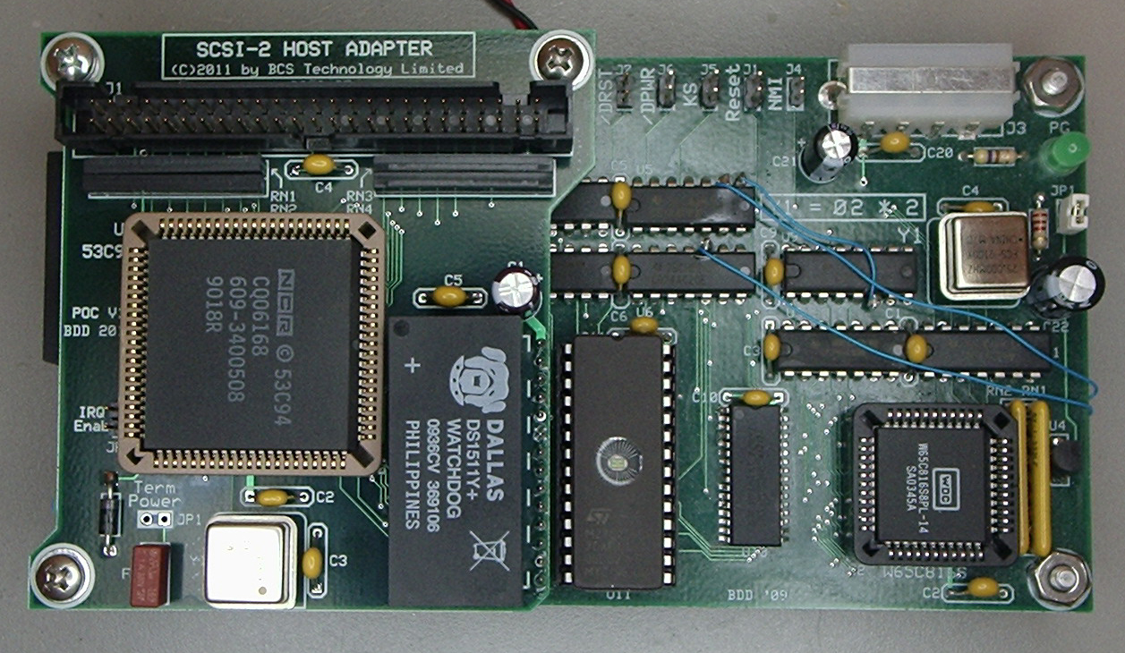
SCSI host adapter has been built and I can talk with the 53C94 controller. I had to slow down the Ø2 clock from 12.5 MHz to 8 MHz to achieve stable operation. The system would boot at the higher Ø2 frequency but was erratic—possibly the result of increase bus loading by the 53C94 (the board runs fine at 12.5 MHz with the 'C94 out of the socket). It's not a concern right now but I will 'scope it later on to see what is going on.
_________________
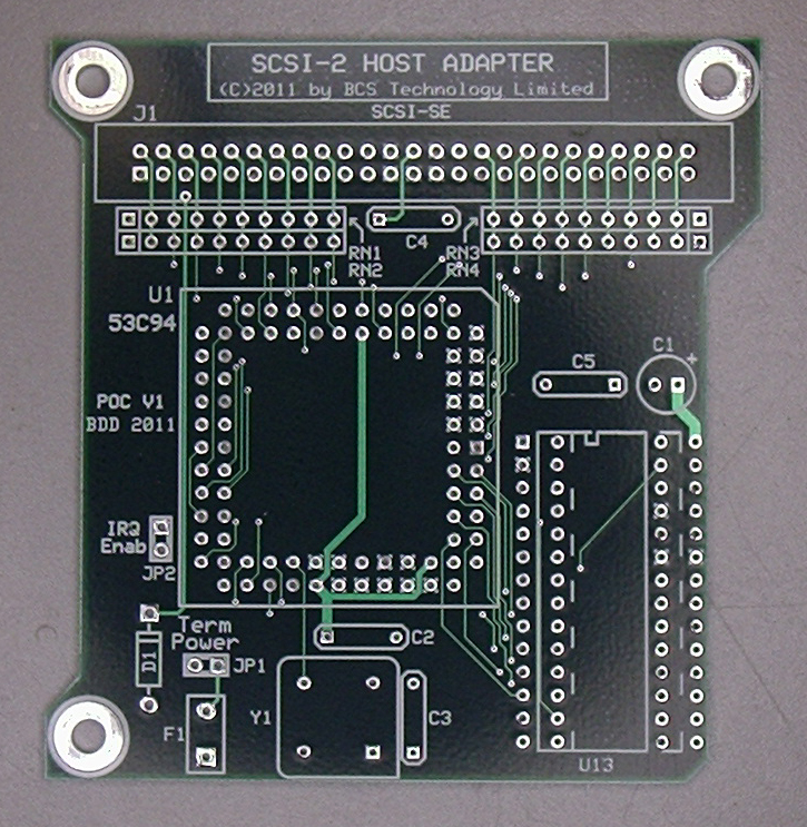
Component side of printed circuit board.
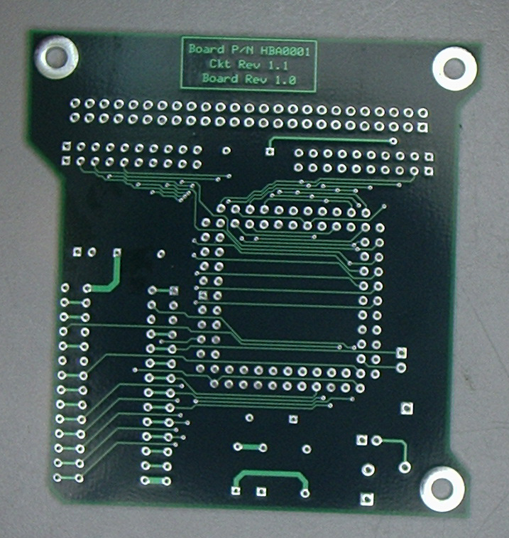
Solder side of printed circuit board.
Test-fitting host adapter PCB to POC board.
Side view of test-fitting host adapter PCB to POC board.
Another view of test-fitting host adapter PCB to POC board.
EIA-232 jacks just fit under the HA's PCB.
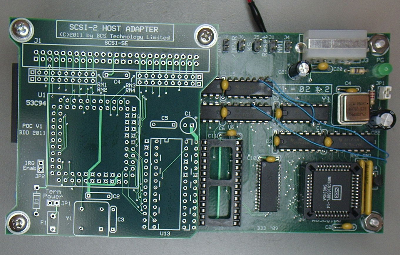
The assembled host adapter. As the HA interfaces to the POC board via the watchdog timer's socket, the watchdog now resides on the HA.
Top view of the host adapter mounted on the POC board.
Another (blurry) view of the finished assembly.
POC Computer Version One
-
BigDumbDinosaur

- Posts: 9428
- Joined: 28 May 2009
- Location: Midwestern USA (JB Pritzker’s dystopia)
- Contact:
SCSI, here we come!
x86? We ain't got no x86. We don't NEED no stinking x86!
-
BigDumbDinosaur
- Posts: 9428
- Joined: 28 May 2009
- Location: Midwestern USA (JB Pritzker’s dystopia)
- Contact:
SCSI Subsystem
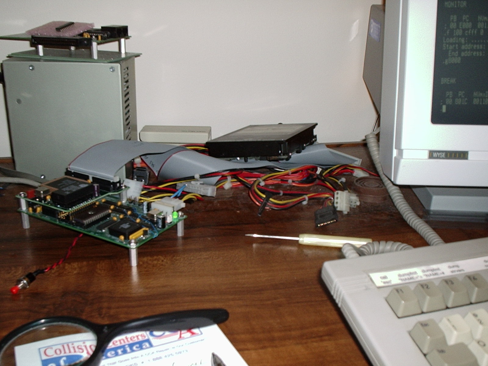
Some SCSI progress is being made. I have written a barebones driver that can query and initialize the 53C94 controller, send a hard reset to the bus and send a "start unit" command to the ancient Seagate ST31230N "Hawk" hard drive that I dragged out of my old computer parts storage.
In contemplating all this, it becomes apparent that a sort of feng shui should be applied to designing the driver. The core functions of getting bytes from or putting bytes on the bus are the same no matter what is going on. However, each of the bus phases requires different processing of those bytes. Data-in, for example, requires that bytes that come in off the bus be stored into a buffer somewhere for later processing. On the other hand, message-in requires that the incoming bytes be used to direct the workflow through the driver. Therefore, it seems the logical approach would be for the driver to consist of modules that are responsible for each bus phase, as well as a module to handle conditions not associated with any one phase (e.g., handling the case where a device is selected but fails to respond).
In order for the correct module to be selected for execution, an IRQ-driven "dispatcher" could be used. As I mentioned, a bus phase change causes an IRQ to be generated. At the same time, the bus phase, which is a three bit binary-encoded value progressing from $00-$07, is available in the 53C94's status register. I'm envisioning that the IRQ handler would, upon determining that the 53C94 has generated a phase change IRQ, would use the phase value as the index into a module address look-up table. Using the 65C816's STA n,S instruction, the IRQ handler would replace the address that was pushed when the IRQ was processed with the address of the new phase module. Upon completion of the IRQ handler, the RTI would send the MPU off to the new module. A similar approach could be used in the case where a 53C94 IRQ is the result of something not involving a bus phase change, such as the aforementioned case where a selected device fails to respond. There are other considerations, of course, but I think that is the fundamental technique that will work.
So it's off to the assembler to write a bit of code!
- My test setup, which is on a desk in my office. This is the "narrow" (eight bit) implementation of the SCSI bus, hence the wide ribbon cable (I agree, it's illogical to have a narrow bus running on a wide cable). Notice how careful I was to cushion the hard drive (the black object roughly in the center of the picture) against the shock of being operated for the first time in some 15 years.

- Status messages emitted by the barebones driver as it configures the SCSI subsystem. The driver starts by performing several tests on the 53C94 to verify that it will respond to commands. The FIFO tests verify that the 16-deep FIFO used to pass bytes to/from the SCSI bus can regurgitate whatever is placed into it. There's also an interrupt test that I currently monitor with the logic probe, as I don't have the 53C94 IRQ line presently tied to the MPU IRQB input. The final step, not shown on the screen, is the issuance of a "start unit" command to the disk, causing it to spin up the platters and recalibrate—complete with assorted noises (SCSI drives of that vintage were not noted for their quietness). With that done, the disk should be ready to accept commands.
Incidentally, the "SCSI initialization failure" message at the top of the picture was emitted by the BIOS during reset, as it doesn't yet know anything about SCSI hardware.
- The SCSI bus has eight operating phases, which can occur in almost any order. For example, the host may request data from a SCSI device. However, following selection, the target device (the old Hawk disk, in this case) may, instead of going to the data-in phase, go to the status phase because it isn't ready to send any data (e.g., the disk isn't spinning). So the driver must be ready for the unexpected and gracefully recover when the target doesn't do as asked.
- The 53C94 will generate an IRQ when the bus changes phase, as well as for other reasons. As SCSI activity involves communication with mechanical devices, this is an essential feature needed to avoid having the MPU twiddle its thumbs until a response occurs to a command. The downside is that the 53C94 cannot be told to not generate interrupts, which initially complicates driver development.
To ease the pain of creating a working driver, I designed the host adapter board so I could isolate the 53C94 from the MPU's /IRQ line. This has allowed me to get the basics out of the way without tripping over spurious IRQs. However, I've reached the point where I will have to allow the 53C94 to interrupt the MPU. Patching code into the system IRQ handler, of course, opens the door to accidental system fatality. Fortunately, there's a conveniently-placed reset button connected to the POC... - The driver must be sufficiently generic in nature that it will work equally well with any SCSI device type. Many SCSI commands are common to all device types, but don't necessarily work in the same fashion in all cases. For example, a read-long command to a disk requires that a 32 bit logical block address (LBA) be passed, as well as the amount of data to be returned. Tapes, on the other hand, can't be addressed by LBA, since they are sequential devices. So flexibility will be key. While I highly doubt I'll be connecting a SCSI document scanner to the POC, a proper driver should, in theory, be able to accommodate one.
- The initiator (host) will arbitrate for bus control and select the target device.
- When the target responds and is ready to proceed, it will take control of the bus and switch it to the command phase.
- The initiator will issue the read command.
- When ready, the target will switch the bus to the data-in phase and send data until the amount requested has been transmitted.
- The target will switch the bus to the status-in phase and send a status byte, normally to indicate that the command was accepted.
- The initiator will read the status byte and act on it as necessary.
- The target will switch the bus to the message-in phase and send a message byte, usually to inform the initiator that the command was completed.
- The initiator will read and act on the message byte as required.
- The target will disconnect from the bus, causing it to go to the bus-free state. The initiator likewise will disconnect, completing the transaction.
In contemplating all this, it becomes apparent that a sort of feng shui should be applied to designing the driver. The core functions of getting bytes from or putting bytes on the bus are the same no matter what is going on. However, each of the bus phases requires different processing of those bytes. Data-in, for example, requires that bytes that come in off the bus be stored into a buffer somewhere for later processing. On the other hand, message-in requires that the incoming bytes be used to direct the workflow through the driver. Therefore, it seems the logical approach would be for the driver to consist of modules that are responsible for each bus phase, as well as a module to handle conditions not associated with any one phase (e.g., handling the case where a device is selected but fails to respond).
In order for the correct module to be selected for execution, an IRQ-driven "dispatcher" could be used. As I mentioned, a bus phase change causes an IRQ to be generated. At the same time, the bus phase, which is a three bit binary-encoded value progressing from $00-$07, is available in the 53C94's status register. I'm envisioning that the IRQ handler would, upon determining that the 53C94 has generated a phase change IRQ, would use the phase value as the index into a module address look-up table. Using the 65C816's STA n,S instruction, the IRQ handler would replace the address that was pushed when the IRQ was processed with the address of the new phase module. Upon completion of the IRQ handler, the RTI would send the MPU off to the new module. A similar approach could be used in the case where a 53C94 IRQ is the result of something not involving a bus phase change, such as the aforementioned case where a selected device fails to respond. There are other considerations, of course, but I think that is the fundamental technique that will work.
So it's off to the assembler to write a bit of code!
-
BigDumbDinosaur
- Posts: 9428
- Joined: 28 May 2009
- Location: Midwestern USA (JB Pritzker’s dystopia)
- Contact:
SCSI Subsystem
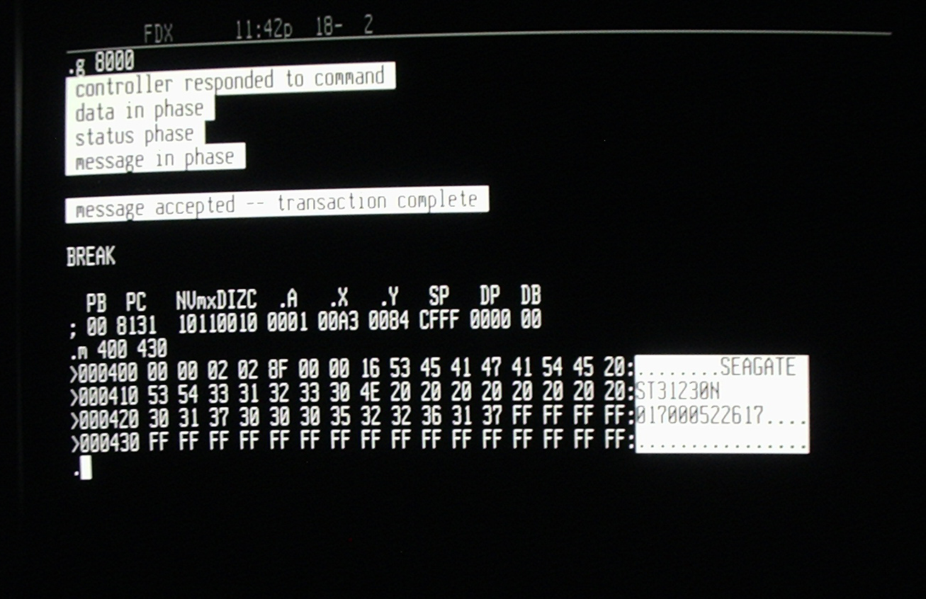
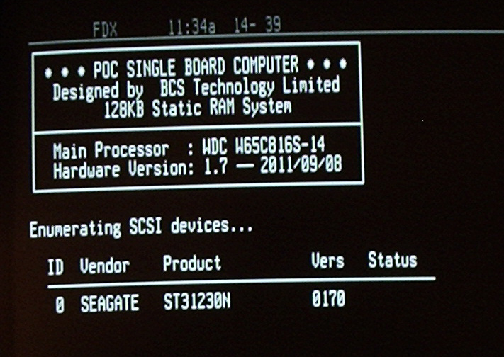
I've written a more elaborate driver for my new host adapter (HBA) and am able to talk to an old Seagate Hawk disk connected to the SCSI port. The memory dump at $000400 indicates this is a Seagate ST31230N model (1.2 GB, for use on an eight bit SCSI bus), with firmware revision 0170 and serial number 00522617.
So far, the driver can interrogate the disk, start/stop it and read a block of data into RAM. Primitive code remaining to be tested is writing to the disk and the disconnect/reconnect feature. Once that is done, the next step will be to "genericize" the driver so it works properly with non-disk peripherals, such as a SCSI DVD drive (of which I have several). Lastly, I'll add the driver to the POC's BIOS ROM so SCSI access is available for future development.
So far, the driver can interrogate the disk, start/stop it and read a block of data into RAM. Primitive code remaining to be tested is writing to the disk and the disconnect/reconnect feature. Once that is done, the next step will be to "genericize" the driver so it works properly with non-disk peripherals, such as a SCSI DVD drive (of which I have several). Lastly, I'll add the driver to the POC's BIOS ROM so SCSI access is available for future development.
-
BigDumbDinosaur
- Posts: 9428
- Joined: 28 May 2009
- Location: Midwestern USA (JB Pritzker’s dystopia)
- Contact:
We got SCSI!
I have completed a working SCSI driver that is now part of the POC unit's BIOS ROM. The driver supports the functionality of both SCSI-1 and SCSI-2, except for tagged command queuing and synchronous data transfer (SDT). SDT requires additional hardware logic that I can't readily establish with POC V1. Other than that, the driver provides all of the primitive functionality required to converse with SCSI devices.
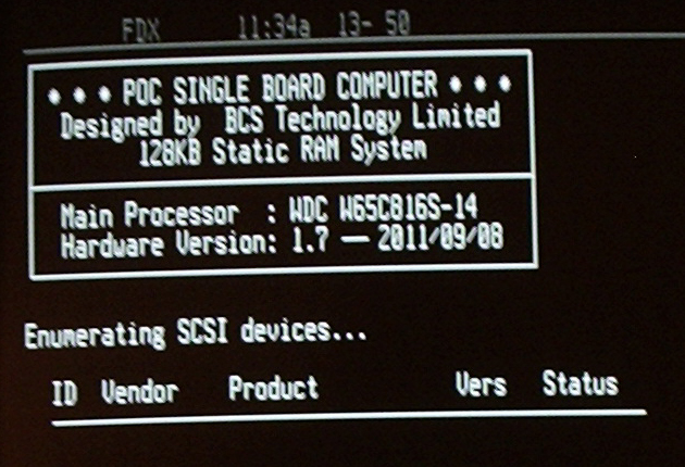
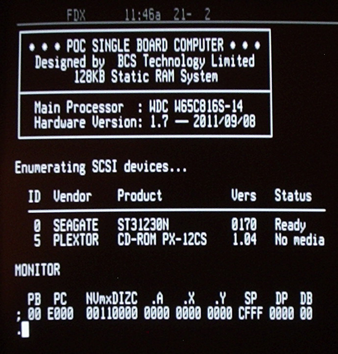
- First step of SCSI enumeration.
At this point, POST has been completed, the SCSI subsystem has been configured and the BIOS is about to poll all possible SCSI IDs for the presence of hardware. As enumeration proceeds, a SCSI device table will be built in RAM for later reference. Key elements of the device table are the device type, block size in bytes and the number of blocks that can be addressed. Multiplying the number of blocks by the block size gives the formatted capacity (bytes) of the device. - SCSI enumeration continues.
Here the old Seagate Hawk hard drive has been detected and is being spun up. The BIOS waits until the drive has reached operating speed and has calibrated to cylinder 0. Once the drive has calibrated, it will report its status. If for some reason, it fails to spin up and calibrate, then a "check condition" status will be reported to the BIOS. - SCSI enumeration completed.
The BIOS has also detected a CD-ROM drive (an old Plextor caddy unit). The CD-ROM doesn't have a disc in it, which is why "No media" was reported. - Memory dump of boot block from the hard drive.
Immediately following enumeration, the BIOS will attempt to load an operating system by copying the boot block on the disk to RAM at $00C900. If the boot block is not recognized as valid, control is turned over to the machine language monitor.
This particular hard drive contains a FAT32 filesystem from the days when I had my UNIX box set up to boot into UNIX or Windows.
-
BigDumbDinosaur
- Posts: 9428
- Joined: 28 May 2009
- Location: Midwestern USA (JB Pritzker’s dystopia)
- Contact:
We have SCSI, but it ain't fast enough!
I've been playing around with the SCSI driver in an effort to make it smaller and faster. Right now I am running the 53C94 controller in PIO mode, which is the only practical mode with the current hardware. PIO is slow...period. The theoretical transfer speed limit with the MPU running at 8 MHz is about 75 KB/sec, and I'm up to about 60 KB/sec (faster if I kill IRQs during a transfer), well below the asynchronous transfer rate of the SCSI bus, which is 3 or 5 MB/sec, depending on the device. The C94 also has a DMA mode, the use of which would substantially reduce the amount of overhead associated with reading and writing each byte. Unfortunately, DMA is not practical with any 65xx system, as no compatible DMA controller apparently exists. However, it appears that it may be possible to set up a quasi-DMA mode with some hardware trickery.
Like most I/O silicon, the C94 has a /CS (chip select) input, R/W inputs (separate, in this case) and some address lines. As is typical, you put an address pattern on A0-A3 (16 possible registers), assert /CS and the MPU is connected to the desired register. One of those registers is a 16-bit FIFO, which is the conduit between the SCSI bus and the MPU's data bus. Bytes written into the FIFO by the MPU are sent to the bus when the C94 is told to send them, and bytes coming in off the bus from the SCSI hardware (e.g., disk) are collected in the FIFO and then made available to the MPU when the C94 is told to collect them and make them available. In PIO mode, the C94 has to be told to send/receive for each byte, using a command sequence that takes between 150 and 200 clock cycles to complete—and that's on top of the code needed to actually read from or write to the FIFO. A standard hard drive block is 512 bytes, so it is easy to see when all the processing time is going (76,800 cycles best case per block).
The FIFO is different from the other C94 registers in that there are two ways to access it. It appears as register $02 when /CS is asserted. However, it is also possible to make the FIFO appear by asserting a separate C94 input called /DACK and not asserting /CS. In such a case, the bit pattern on the address bus is completely ignored and the FIFO is connected to D0-D7, just as it would if $02 appeared on the address bus and /CS had been asserted.
Unfortunately, the 53C94 data sheet that I followed in designing the host adapter and writing the driver does a poor job of explaining how this all works. Since I couldn't understand what the author of the data sheet was trying to explain, I settled for using PIO mode. However, I recently came across a copy of the data sheet for the C94's immediate ancestor, the NCR 53C90, in which a much better job of explaining the controller's DMA features and how it responds to the DMA control input and output can be found. So now I'm revisiting my host adapter design to see if I can use the DMA features to improve performance. My vague thinking at this point is to somehow make the MPU seem to be a DMA controller.
I already mentioned the /DACK input, which when asserted, causes the FIFO to connect to the data bus without regard to what is on the address bus. /DACK has a companion output, DREQ, which when asserted by the C94, tells external hardware that data is waiting in the FIFO during read mode, or that there is room in the FIFO for another byte during write mode. So, the theory in my little dinosaur brain goes, if I can get the MPU to see when DREQ has been asserted, then the MPU could assert DACK and grab a byte from the FIFO and store it in RAM (read mode), or grab a byte from RAM and put it in the FIFO (write mode). Since the SCSI bus runs at a high rate of speed (faster than the MPU can physically move bytes to and from the FIFO), and since DREQ changes state as fast as the C94 and SCSI bus can operate, the performance limit would now be a matter of high tightly can I code the I/O loop that polls DREQ, toggles /DACK and services the FIFO.
Toggling /DACK to get access to the FIFO isn't too difficult. What I would need is some glue logic that would assert /CS if the C94 is selected and the register number on A0-A3 is anything other than $02. The same logic would assert /DACK if the C94 is selected and the register number is $02. It can be done with discrete gates, but a PLD would be much faster. However, for proof of concept testing, I could do it with some 74ABT or 74F logic, which wouldn't add too much propagation delay.
DREQ is more problematic. If my POC unit were powered by the 65C02, I could tie DREQ to the MPU's SOB (set overflow) input through an inverter, which would be easily monitored with a BIT instruction. However, the 816 doesn't have SOB. So I would have to somehow make the DREQ output appear to be a bit on the data bus when a specific memory location was checked. It seems something like a 74ABT574 octal D-flop could do this, as it has very short prop time and can be tri-stated when the MPU is not looking at DREQ. I think I could tie the 574's /OE input through an inverter to A4 (which is not connected to the C94) and when the C94 I/O range is selected with $10 on the address bus, the 574 would strobe the state of DREQ to, say, D7 for easy testing with a BIT instruction.
What would be really cool, but definitely a project for another time, would be to figure out how to rig up a 65C02 to act as a DMA controller. That's a topic for another day. For now, I'm going to cogitate a bit and see if I can synthesize the DMA stuff with some gates and such.
Oh, one more thing, as Columbo would have said. It may be that watching DREQ is not necessary, as it appears the C94 and the SCSI bus would be waiting on the MPU, not the other way around.
-----
Edit: /DREQ is supposed to be DREQ.
Last edited by BigDumbDinosaur on Wed Oct 12, 2011 1:56 am, edited 1 time in total.

BigDumbDinosaur wrote:
My vague thinking at this point is to somehow make the MPU seem to be a DMA controller.
Briefly, Lancaster's "cheap video" simulates a DMA controller using the CPU. The CPU's PC register is used for the DMA addresses. To output (or input) a video scan line (disk sector), the CPU does a JSR to where the data is stored! But the busses get isolated and (say) 511 NOP instructions and one RTS get fed to the CPU, while the 512 data bytes get fed to the video shift register (C94 FIFO).
Obviously there's some hanky-panky required to orchestrate this little scam, but the complexity is less than you might at first suppose. Lancaster arranged things so that access to a dedicated portion of the address space -- a redundant image of the data buffer -- would simultaneously enable the phony NOPs and the data transfers. And you have lots of address space available since your host is an '816, right?
Sorry for the rather terse explanation. And I'm not tryna "sell" you on the idea, BDD... just thought I'd throw it into the mix, for amusement if nothing else. Maybe it'll stimulate some random thought that leads you to another approach altogether.
cheers,
Jeff
P.S.:
- to clarify, in case anyone's interested: decoding is such that, within the extra image of the buffer, two memories both become selected. A small PROM (or random logic) may be used to feed the bogus NOPs and RTS directly to the CPU. Data from main memory never reaches the CPU because a tri-state buffer isolates the main memory bus from the CPU bus. (The address bus is not tri-stated.)
- the NOP/RTS mix in the example is really 510 cycles and 2, not 511 and 1. (The explanation above is simplified slightly.) Cycle-by-cycle behavior of the 65xx dictates that RTS will account for two cycles because the CPU always fetches the byte following any op-code.
- instead of NOP instructions, CMP Immediate instructions may be preferable (or any Immediate opcode). This doubles the bandwidth (ie, increment rate on the address bus), since NOP occupies 1 byte and consumes 2 cycles, whereas an Immediate instruction occupies 2 bytes and consumes 2 cycles. Thus the simulated DMA can operate as quickly as 1 byte per clock.
PPS- I've added a page on my web site that deals with this subject.
Last edited by Dr Jefyll on Fri Oct 25, 2019 4:21 am, edited 2 times in total.
-
BigDumbDinosaur
- Posts: 9428
- Joined: 28 May 2009
- Location: Midwestern USA (JB Pritzker’s dystopia)
- Contact:
SCSI "DMA"
Dr Jefyll wrote:
BigDumbDinosaur wrote:
My vague thinking at this point is to somehow make the MPU seem to be a DMA controller.
Briefly, Lancaster's "cheap video" simulates a DMA controller using the CPU. Ie; the CPU's PC register is used for the DMA addresses. To output (or input) a video scan line (disk sector), the CPU does a JSR to where the data is stored! But the busses get isolated and (say) 511 NOP instructions and one RTS get fed to the CPU, while the 512 data bytes get fed to the video shift register (C94 FIFO).
Obviously there's some hanky-panky required to orchestrate this little scam, but, when you actually look at it, the complexity is less than you might at first suppose. Lancaster used a dedicated portion of the address space -- a redundant image of the data buffer -- to cue the phony NOPs. And you have lots of address space available since your host is an '816, right?
Sorry for the rather terse explanation. And I'm not tryna "sell" you on the idea, BDD... just thought I'd throw it into the mix, for amusement if nothing else. Maybe it'll stimulate some random thought that leads you to another approach altogether.
cheers,
Jeff
The solution? Connect /DACK to an unused output on the 'AC138 I/O decoder. That's all there is to it. If I address any address in that I/O page the FIFO appears on the data bus.
Total hardware required: 3 inches of wirewrap wire and two drops of solder.
Re: SCSI "DMA"
BigDumbDinosaur wrote:
Actually, I stumbled over a stupidly simple solution. [...] Total hardware required: 3 inches of wirewrap wire and two drops of solder.
Quote:
The SCSI bus runs faster than the MPU can physically process bytes.
Quote:
What would be really cool, but definitely a project for another time, would be to figure out how to rig up a 65C02 to act as a DMA controller. That's a topic for another day.
-- Jeff
-
BigDumbDinosaur
- Posts: 9428
- Joined: 28 May 2009
- Location: Midwestern USA (JB Pritzker’s dystopia)
- Contact:
Re: SCSI "DMA"
Dr Jefyll wrote:
BigDumbDinosaur wrote:
The SCSI bus runs faster than the MPU can physically process bytes.
Let's suppose the system is reading from a disk. Let's also suppose I'm running the bus at the SCSI-1 asynchronous rate, which is the slowest possible rate. That's 3.5 MB/sec on the bus. As the bytes come in, keeping in mind they are arriving at 285 nanosecond intervals, they collect into the FIFO, which holds 16 of them. The MPU has to read the FIFO one byte at a time and then store each byte into a buffer.
An absolute, nonindexed 8 bit read operation requires four clock cycles, or 500 nanoseconds with an 8 MHz Ø2 clock (the current speed I'm using). So in reading the FIFO the first time the MPU will already behind the bus. Even if I could step Ø2 up to 20 MHz (I can't with this design), I'd still be looking at 200ns for the read operation, which is slightly ahead of the bus. However, storing the byte will cost me at least five clock cycles. At 20 MHz, I wouldn't be able to keep up with the bus anyhow, as I'd be consuming 900ns per byte to fetch and store—and that's not accounting for loop overhead, as well the effects of servicing IRQs.
Now, a true DMA controller could (in theory) grab bytes as fast as they come in, because DMA controllers typically move a byte on each clock cycle. Even the controller that was in the Commodore 1750 "RAM expander" could move 1 MB/sec, which was the I/O clock rate in the C-64 and C-128. However, since I don't have a real DMA controller, the best I can do is code my fetch/store loop as tightly as possible.
Incidentally, not being able to keep up with the bus while running in asynchronous mode will not cause any problems, such as a data overrun. In async mode, each byte placed on the bus by the sending device has to be ACKed by the receiving device (e.g., the 'C94). When the FIFO is full, the 'C94 will stop ACKing the sending device, which will not send another byte until the previous one has been ACKed. It's analogous to CTS-RTS flow-control between two EIA-232 devices.
Re: SCSI "DMA"
BigDumbDinosaur wrote:
Incidentally, not being able to keep up with the bus while running in asynchronous mode will not cause any problems, such as a data overrun. In async mode, each byte placed on the bus by the sending device has to be ACKed by the receiving device (e.g., the 'C94). When the FIFO is full, the 'C94 will stop ACKing the sending device, which will not send another byte until the previous one has been ACKed. It's analogous to CTS-RTS flow-control between two EIA-232 devices.
Quote:
Now, a true DMA controller could (in theory) grab bytes as fast as they come in, because DMA controllers typically move a byte on each clock cycle.
That's what the Lancaster approach does -- move a byte every clock cycle. The reason I mentioned it is because you mentioned thinking about some sort of DMA.
As for how it works, I admit I find it tough to explain, even though it's actually quite simple. Earlier tonight I edited my original post (Mon Oct 10), hoping to shed some light on the matter, but maybe I've missed mentioning some key point -- you know how it is. So questions are welcome.
-- Jeff

BigEd wrote:
could you put together a new head post on Lancaster-style DMA?
BigEd wrote:
the operand can be the same as the opcode, so it's no more complex
-- Jeff
-
BigDumbDinosaur
- Posts: 9428
- Joined: 28 May 2009
- Location: Midwestern USA (JB Pritzker’s dystopia)
- Contact:
POC
Well, it's been close to three months since I last powered POC V1. Just for grins, I flipped the switch. The unit ran through POST and the SCSI hardware all checked in. For some reason, the date and time are way off. Something had to have tinkered with the watchdog with an improper write operation. Hmmm...a new hardware problem or a bug in the BIOS code?
x86? We ain't got no x86. We don't NEED no stinking x86!
-
BigDumbDinosaur
- Posts: 9428
- Joined: 28 May 2009
- Location: Midwestern USA (JB Pritzker’s dystopia)
- Contact:
POC V1
fachat wrote:
Or the usual problem - drained BIOS battery? 
I checked the "battery good" bit in the watchdog's status register (has a built-in lithium ion battery) and it is set, meaning the battery voltage is in range. I reset all the clock registers and loaded a data pattern into NVRAM (256 bytes), powered down and disconnected the unit from the power supply. I'll come back to it in a few days and see if anything has changed.
x86? We ain't got no x86. We don't NEED no stinking x86!