8BIT wrote:
ElEctric_EyE, Any progress on your trouble?
Did you see the suggestions Lee and I gave?
If you can post a little more of the schematic (or a link to it), it would help.
Daryl
Did you see the suggestions Lee and I gave?
If you can post a little more of the schematic (or a link to it), it would help.
Daryl
8BIT wrote:
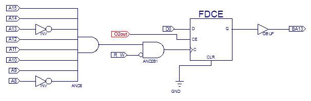
From the schematic, it looks like a write to DExx loads the upper address bytes. Is this the "bank" variable referenced in your code?
...
Daryl
...
Daryl
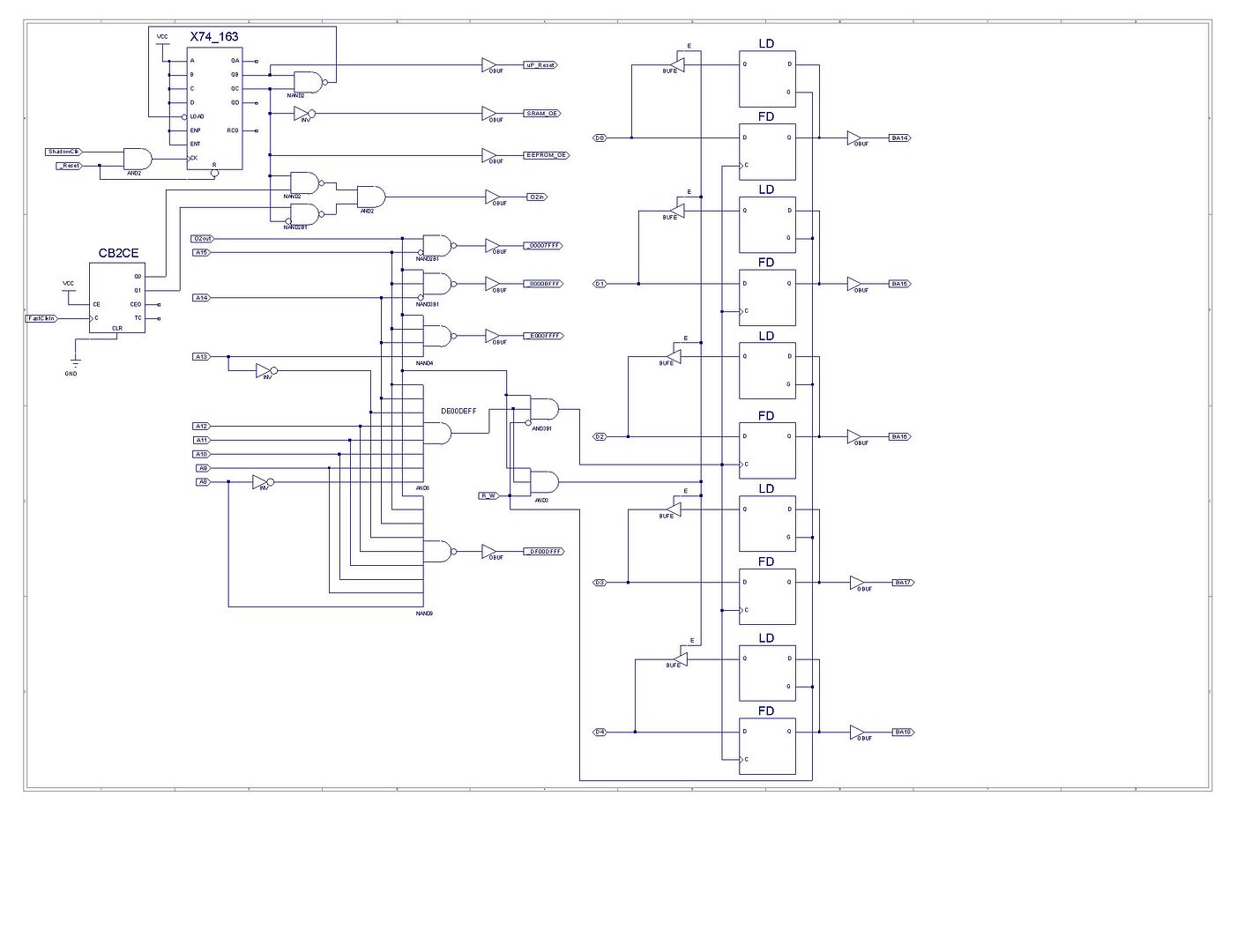
Here's the updated schematic (I am trying to use a new (.emf) format so the pic will fit into whatever size screen or CRT you are using).
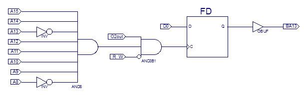
Edit: The .emf format is not supported by photobucket, sorry for the large pic, but I am tired, soon off to bed. Thanks for the sugg's. I'll work on the pic size... In the schematic below "FD" is a D-type flip flop (like a 74374), and "LD" is a D-type latch (like a 74373), except the clock on "FD" latches the data on the rising edge, and the data on "LD" is transparent on a high "G". Also the tri-state BUFE's on the output of the "LD" latches are active high...
fachat wrote:
...Did not have a close look, but this looks like 8bit code to me. Did you try to put the X/Y registers in 16bit mode and use 24bit absolute address code? Makes such loops much simpler.
André
André