6502.org Forum  Projects  Code  Documents  Tools  Forum
It is currently Sat Sep 28, 2024 10:23 am

All times are UTC


Post new topic Reply to topic  [ 297 posts ]  Go to page Previous  1 ... 8, 9, 10, 11, 12, 13, 14 ... 20  Next
Author Message
 Post subject:
PostPosted: Tue Apr 06, 2010 2:08 pm 
Offline

Joined: Tue Jul 05, 2005 7:08 pm
Posts: 1041
Location: near Heidelberg, Germany
ElEctric_EyE wrote:
This is the software to copy the 512K EEPROM to 512 SRAM. Seems to be getting stuck here. If I comment out this part the program progresses... My mind is in hardware mode, maybe someone can help me out here. What am I missing? I'm sure it's software related...


Did not have a close look, but this looks like 8bit code to me. Did you try to put the X/Y registers in 16bit mode and use 24bit absolute address code? Makes such loops much simpler.

André


Top
 Profile  
Reply with quote  
 Post subject:
PostPosted: Sat Apr 10, 2010 12:28 am 
Offline
User avatar

Joined: Fri Aug 30, 2002 9:02 pm
Posts: 1738
Location: Sacramento, CA
ElEctric_EyE, Any progress on your trouble?

Did you see the suggestions Lee and I gave?

If you can post a little more of the schematic (or a link to it), it would help.

Daryl


Top
 Profile  
Reply with quote  
 Post subject:
PostPosted: Sat Apr 10, 2010 1:25 am 
Offline

Joined: Mon Mar 02, 2009 7:27 pm
Posts: 3258
Location: NC, USA
8BIT wrote:
ElEctric_EyE, Any progress on your trouble?

Did you see the suggestions Lee and I gave?

If you can post a little more of the schematic (or a link to it), it would help.

Daryl


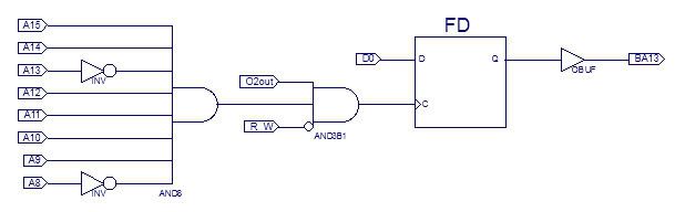
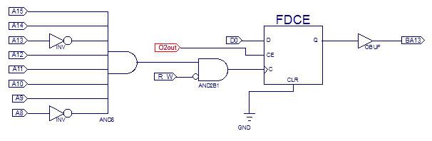
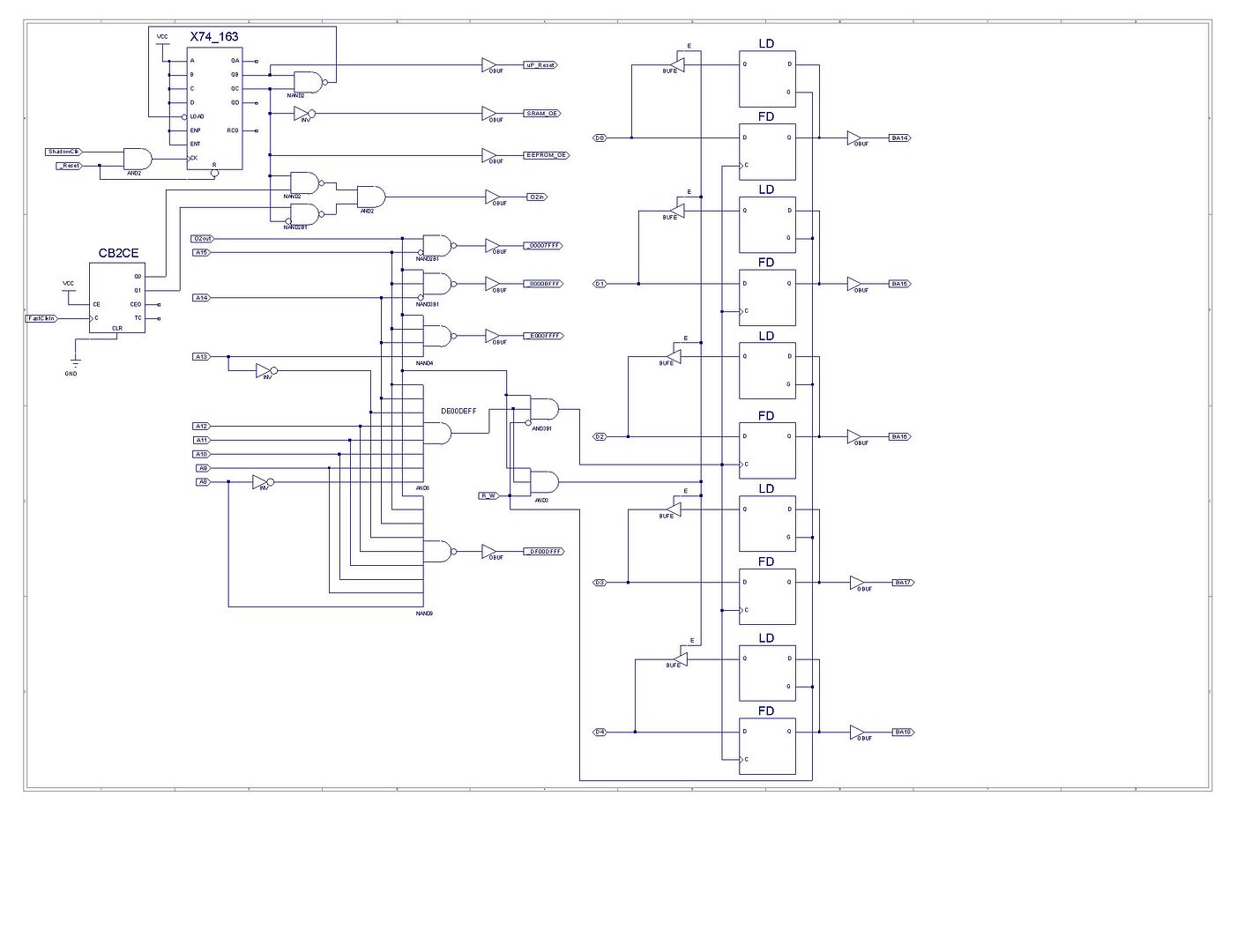
I have taken Leeeeee's suggestion to mirror the write-only register with a zero page register. The loop reads and writes to the zero page reg and then writes to the register inside the CPLD too, Doesn't work. In fact the 5 bit flip flop inside the CPLD is not being written to correctly, ever. I'm focusing now on this issue. The divider clocks in the CPLD are working fine... I've got the display to do a reset and clear. The bank circuit is not working. The previous schematic has only the flip flop (output/write to only), and phase 2 is also being used earlier in the logic path, instead of where it should be, at the very last stage of decoding. I've taken care of that as well in the next schematic, but it still isn't working. Before I start banging my head against the wall, I am going to start the latest schematic from scratch. I went through this process before and all of a sudden the circuit worked... A Xilinx software issue or maybe I'm closing down the software incorrectly...

8BIT wrote:
From the schematic, it looks like a write to DExx loads the upper address bytes. Is this the "bank" variable referenced in your code?
...
Daryl

The 5 bit bank Reg is @ $DE00 and is mirrored through $DEFF. The 16K window the 65C02 sees (into 512K) is from $8000-$BFFF. In order for this part of my software to work correctly the bank Reg has to be #$00. I have the character fonts and character string data there (They used to be from $F000-$FFF9 on the 8K OS EEPROM.)


Here's the updated schematic (I am trying to use a new (.emf) format so the pic will fit into whatever size screen or CRT you are using).

Edit: The .emf format is not supported by photobucket, sorry for the large pic, but I am tired, soon off to bed. Thanks for the sugg's. I'll work on the pic size... In the schematic below "FD" is a D-type flip flop (like a 74374), and "LD" is a D-type latch (like a 74373), except the clock on "FD" latches the data on the rising edge, and the data on "LD" is transparent on a high "G". Also the tri-state BUFE's on the output of the "LD" latches are active high...

Image

fachat wrote:
...Did not have a close look, but this looks like 8bit code to me. Did you try to put the X/Y registers in 16bit mode and use 24bit absolute address code? Makes such loops much simpler.

André


Sounds like the 65816? I have zero experience with that CPU, Andre. This is strictly WDC65C02 at this point.

_________________
65Org16:https://github.com/ElEctric-EyE/verilog-6502


Top
 Profile  
Reply with quote  
 Post subject:
PostPosted: Sat Apr 10, 2010 5:21 am 
Offline
User avatar

Joined: Fri Aug 30, 2002 9:02 pm
Posts: 1738
Location: Sacramento, CA
Ok, I was actually wanting a schematic that shows the rest of the circuit - including the CPU, RAM, EEPROM, and CPLD.

As I understand, you want to run the CPU slowly, read an EEPROM and copy it into RAM, using banking to control a window to allow access to >64k. Once done, you want to up the speed and run purely from RAM.

I understand your gating inside the CPLD. It seems as if the LD's can be replaced with a simple tri-state buffer, as the Q outputs of the FD's will always be stable during a read.

I am interested in how exactly the CPU address lines connect to the SRAM.

Is there a multiplexer connected between them to gate the bank register only during accesses to the window ($8000-BFFF)?

If the bank register shown is connected directly to the RAM upper address pins, them I see a huge problem with access to RAM outside the window with the bank register non-zero.

I can explain more if my assumptions are correct.

Daryl


Top
 Profile  
Reply with quote  
 Post subject:
PostPosted: Sat Apr 10, 2010 10:30 pm 
Offline

Joined: Mon Mar 02, 2009 7:27 pm
Posts: 3258
Location: NC, USA
Yes, that is exactly what I am trying to do. Copy the EEPROM to SRAM when running @3.5 MHz, then (for now) running @7Mhz directly from the SRAMs, and your assumption is correct. My A0-A13 address lines are connected from the CPU to the 512K SRAM/EEPROMs, addressing the 16K window. Which window is controlled by the 5 bit flip-flop and has lone control over A14-A18. How would there be a problem when these upper address lines are stable way before the others? (And thanks for your insight into not needing the latches)
I have the schematic posted in this link: viewtopic.php?t=1503&start=75 (it's the last schematic posted, some of the clock signals have changed, but the basic addressing is the same). I tried to put the data and address lines on the same horizontal level, so you can infer that they are connected. I plan on using the Eagle CAM software others have mentioned here, when I am closer to having boards made, which hopefully won't be much longer. Again, thanks for your help 8bit!

_________________
65Org16:https://github.com/ElEctric-EyE/verilog-6502


Top
 Profile  
Reply with quote  
 Post subject:
PostPosted: Sat Apr 10, 2010 11:14 pm 
Offline
User avatar

Joined: Fri Aug 30, 2002 1:09 am
Posts: 8520
Location: Southern California
Quote:
Sounds like the 65816? I have zero experience with that CPU, Andre. This is strictly WDC65C02 at this point.

You can make the board able to take either the '02 or the '816 with jumper options to make the choice. Most of the pins are the same. The '816, although appearing mysterious and distant and daunting to the newcomer, really does make a lot of things easier, not harder. You'll never regret going to it. You can initially use the '816 like an '02, then venture into its extra capabilities slowly. It is not necessary to latch, decode, or use its high address byte to take advantage of it, although in your case, since you want more than 64K memory space, it would definitely improve things.


Top
 Profile  
Reply with quote  
 Post subject:
PostPosted: Sun Apr 11, 2010 4:32 am 
Offline
User avatar

Joined: Fri Aug 30, 2002 9:02 pm
Posts: 1738
Location: Sacramento, CA
ElEctric_EyE wrote:
Yes, that is exactly what I am trying to do. Copy the EEPROM to SRAM when running @3.5 MHz, then (for now) running @7Mhz directly from the SRAMs, and your assumption is correct. My A0-A13 address lines are connected from the CPU to the 512K SRAM/EEPROMs, addressing the 16K window. Which window is controlled by the 5 bit flip-flop and has lone control over A14-A18. How would there be a problem when these upper address lines are stable way before the others? (And thanks for your insight into not needing the latches)
I have the schematic posted in this link: viewtopic.php?t=1503&start=75 (it's the last schematic posted, some of the clock signals have changed, but the basic addressing is the same). I tried to put the data and address lines on the same horizontal level, so you can infer that they are connected. I plan on using the Eagle CAM software others have mentioned here, when I am closer to having boards made, which hopefully won't be much longer. Again, thanks for your help 8bit!

OK, I just didn't look back far enough. Thanks. And I was assuming you were using just one RAM chip. Now that I see the big picture, my thoughts about the need for a multiplexer were wrong.

I'll take another look.

hope its something simple.

Daryl


Top
 Profile  
Reply with quote  
 Post subject:
PostPosted: Sun Apr 11, 2010 11:29 am 
Offline

Joined: Mon Mar 02, 2009 7:27 pm
Posts: 3258
Location: NC, USA
So, if it's agreed the concept is solid, I am going to assume it's something with the Xilinx software. I ran into this before, where I had to re-input the whole schematic fresh. The netlists or something else in ISE gets screwy after many modifications to the schematic in between shutting the program down. I'll try it tonight after work and report back..

GARTHWILSON wrote:
... The '816, although appearing mysterious and distant and daunting to the newcomer, really does make a lot of things easier, not harder. You'll never regret going to it. You can initially use the '816 like an '02, then venture into its extra capabilities slowly. It is not necessary to latch, decode, or use its high address byte to take advantage of it, although in your case, since you want more than 64K memory space, it would definitely improve things.


That's not totally out of the question, I do have 2 40-pin DIP versions. But for right now I have to try to keep things as simple as possible. Also I read one of your posts from years ago that the WDC65C02 is capable of 24MHz operation. This is actually what I am shooting for, when I get the new 50MHz 640x480 display in June (it's backordered).

Also I have some ideas of using another CPLD to do hardware drawing, but that's for much later...

_________________
65Org16:https://github.com/ElEctric-EyE/verilog-6502


Top
 Profile  
Reply with quote  
 Post subject:
PostPosted: Sun Apr 11, 2010 3:26 pm 
Offline
User avatar

Joined: Fri Aug 30, 2002 1:09 am
Posts: 8520
Location: Southern California
Quote:
Also I read one of your posts from years ago that the WDC65C02 is capable of 24MHz operation. This is actually what I am shooting for

I know 65816's have been run at 20MHz in a production product too, and a 20MHz '816 will get a job done much faster than a 24MHz '02, assuming the programming is done so as to take advantage of the 816's added capabilities.


Top
 Profile  
Reply with quote  
 Post subject:
PostPosted: Mon Apr 12, 2010 10:27 pm 
Offline

Joined: Tue Jul 05, 2005 7:08 pm
Posts: 1041
Location: near Heidelberg, Germany
ElEctric_EyE wrote:
8BIT wrote:
fachat wrote:
...Did not have a close look, but this looks like 8bit code to me. Did you try to put the X/Y registers in 16bit mode and use 24bit absolute address code? Makes such loops much simpler.

André


Sounds like the 65816? I have zero experience with that CPU, Andre. This is strictly WDC65C02 at this point.


Yes, that's what I meant. I'd recommend using at least the 65802 - 16 bit modes make some things much easier.

André


Top
 Profile  
Reply with quote  
 Post subject:
PostPosted: Mon Apr 12, 2010 10:33 pm 
Offline

Joined: Tue Jul 05, 2005 7:08 pm
Posts: 1041
Location: near Heidelberg, Germany
ElEctric_EyE wrote:
So, if it's agreed the concept is solid, I am going to assume it's something with the Xilinx software. I ran into this before, where I had to re-input the whole schematic fresh. The netlists or something else in ISE gets screwy after many modifications to the schematic in between shutting the program down. I'll try it tonight after work and report back..


In my 6502 replacement card I'm using a Xilinx CPLD as well and I am currently having trouble debugging it. But I found this
http://mbmn.net/uer/tutorials/vhdl-with-ghdl/
tutorial about the simulation, and managed to get the test work - so I'm going to try it with my design as well.

Basically you write a "testbench" VHDL, with something like "set signal A to 1, wait 100ns, set signal A to 0, wait 100ns, start over" to generate input, connect that with your device and view the output signals with the GTKWave viewer (all on Linux though, and installation requires some compilation) But I hope to find out what's wrong with my design.

André


Top
 Profile  
Reply with quote  
 Post subject:
PostPosted: Mon Apr 12, 2010 10:44 pm 
Offline
User avatar

Joined: Fri Aug 30, 2002 1:09 am
Posts: 8520
Location: Southern California
Quote:
I'd recommend using at least the 65802

I don't know where you'll find one though, unless you rob me. They're not in production anywhere anymore AFAIK.


Top
 Profile  
Reply with quote  
 Post subject:
PostPosted: Tue Apr 13, 2010 3:48 pm 
Offline

Joined: Mon Mar 02, 2009 7:27 pm
Posts: 3258
Location: NC, USA
I re-inputted the schematic with the same non-working result... So, to test my wiring and software, I removed the flip-flop and internally grounded all the banked adress lines instead of using the flip-flops, and it worked great, which proves my wiring and software to be working.
So I am thinking it's not as easy as it looks to program a CPLD, even using just schematics. To program a data latch or flip-flop I suspect ISE needs a proper constraints file to group circutis together for a register. Even so, all the flip-flops are set to have an initial 'start-up' output of logic '0', but they're not which is another question mark. I've been working with the constraints editor, but there are so many options, I'm trying to get some headway by posting in the Xilinx forums. I'll have to be persistent, heh :wink: It's probably like asking where my ass is supposed to be.

_________________
65Org16:https://github.com/ElEctric-EyE/verilog-6502


Top
 Profile  
Reply with quote  
 Post subject:
PostPosted: Thu Apr 15, 2010 12:20 am 
Offline

Joined: Mon Mar 02, 2009 7:27 pm
Posts: 3258
Location: NC, USA
No need to worry about constraint files yet, looks like a can of worms. Turns out I was not using the correct flip-flop.

Got a quick response from Xilinx forums here: http://forums.xilinx.com/xlnx/board/mes ... ad.id=1467

I was having a problem with addressing a flip-flop, actually 5 flip-flops for the banked address. I thought the logic was good, but 2 guys on the forum pointed out I was using a gated clock, apparently not a good idea. To simplify, using 1 flip-flop, this is what I was trying to do:
Image

They suggested I do this, which does work (WOOO!)
Image

Logically I think my original circuit should have worked in the real world using discrete TTL. What do you all think about this?

_________________
65Org16:https://github.com/ElEctric-EyE/verilog-6502


Top
 Profile  
Reply with quote  
 Post subject:
PostPosted: Thu Apr 15, 2010 7:43 pm 
Offline

Joined: Thu Jul 26, 2007 4:46 pm
Posts: 105
I'm not so sure that it would normally be accepted by TTL; it would all depend upon the setup and hold times. In general, using the internal logic element's clock enable is always preferable; it is designed to deal with jitter better than the logic elements clock pin.

If you must employ clock gating without the device's support, it is recommended that you always synchronize the stopping and starting phase, to avoid any too-short clock pulses.

By the way, are you sure you're supposed to be running the clock to the clock enable pin, and the enable to the clock pin?


Top
 Profile  
Reply with quote  
Display posts from previous:  Sort by  
Post new topic Reply to topic  [ 297 posts ]  Go to page Previous  1 ... 8, 9, 10, 11, 12, 13, 14 ... 20  Next

All times are UTC


Who is online

Users browsing this forum: No registered users and 42 guests


You cannot post new topics in this forum
You cannot reply to topics in this forum
You cannot edit your posts in this forum
You cannot delete your posts in this forum
You cannot post attachments in this forum

Search for:
Jump to: