Page 11 of 15
Posted: Sat Apr 02, 2011 5:52 pm
by Arlet
The 'IR' value is not a register, and it usually reflects the DI (Data In) bus. Only in the DECODE state is the IR equal to the opcode (and that's the only time the IR value is inspected).
You can visualize the state in the waveform viewer by including the 'statename' signal from the cpu.v module. Note that the 'statename' signal isn't enabled by default. You'll have to predefine the debug symbol 'SIM', or remove this line from cpu.v:
`ifdef SIM
and the corresponding :
`endif
When you add the 'statename' variable to the waveform viewer, make sure you set the radix to ASCII, because it's a text string.
Posted: Sat Apr 02, 2011 6:56 pm
by ElEctric_EyE
I thought it stood for Instruction Register...
I did what you said, I commented out line 221 and 285.
Got a compiler error on line 283; 'A','X','Y','S' has not been declared.
Posted: Sat Apr 02, 2011 7:10 pm
by Arlet
You'll need to remove the same `ifdef/`endif here.
Code: Select all
`ifdef SIM
wire [7:0]   A = AXYS[SEL_A];           // Accumulator
wire [7:0]   X = AXYS[SEL_X];           // X register
wire [7:0]   Y = AXYS[SEL_Y];           // Y register
wire [7:0]   S = AXYS[SEL_S];           // Stack pointer
`endif
That will also allow you to add A, X, Y, and S to the waveform.
Yes, IR means Instruction Register, because I took that from the 6502 block diagram, but there wasn't enough time to use a real register.
Posted: Sat Apr 02, 2011 9:16 pm
by ElEctric_EyE
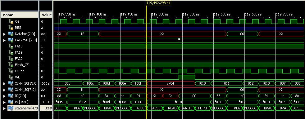
Oh nice! Here (below) is where the problem is occurring. During the second INC $C004, FA18 should go low, and FA19 should go high. It looks like the address isn't decoding properly? Sorta doesn't make sense because it works the first time. Let me explain my signals.
O2 is before the DCM. Constrained at 20.58ns.
O2Int is after the DCM. For simulation purposes, I kept it at a 4:5 ratio, i.e. 38.8MHz. It is present to the CPU, internal synchronous RAM, and internal synchronous ROM.
WE is from the 6502 core.
XLXN_20[15:0] is the address bus Net present to everything internally.
XLXN_30[7:0] is the DataOut from the 6502 core. It goes to the internal RAM, ROM, the FA17to10 FD8CE, the FA25to18 FD8CE (lower 3 bits used). and then finally out to the world through an OBUF8. After which it becomes Databus[7:0].
I initially posted today because I was worried I may have hit that instance (or something similar) in which I would have to use a DDR flip flop
as mentioned on your homepage Arlet. But I see now, that is only write/write situation, not applicable here.
Anyway, thanks for helping me along!
In due time I will figure it out.

Posted: Sun Apr 03, 2011 6:42 am
by Arlet
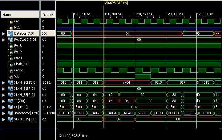
Maybe I'm not understanding the schematics properly, but it looks like your $C004 location is write-only, so the INC instruction wouldn't work.
When reading from memory, the result should be provided on the DI bus 1 cycle after the RE is asserted. That's how the block RAMs do it, and that's what you should mimic if you want to have your own readable memory locations.
Posted: Sun Apr 03, 2011 4:20 pm
by ElEctric_EyE
Maybe I'm not understanding the schematics properly, but it looks like your $C004 location is write-only, so the INC instruction wouldn't work.
Those are old/incorrect schematics. I could've corrected them, but decided against that. I'll post updated ones when I get this working. I shouldn't have posted any schematics at all until I was sure it was working...
Speaking of schematics, now when I think I have a solid design, I like to re-input the whole project from scratch as proof for myself. I like to create a new project, copy the schematic files(.sch) and the 6502 core verilog files(.v) then remake the symbols. Then open up the top-level schematic and update the symbols. For the RAM & ROM I copy nothing, I remake those from scratch, which isn't too difficult... But I digress!
Right now I have each output of the 2 FD8CE FF's going to a 2to1 MUX that selects a '0' when inactive or 'data' when active. The output of each MUX goes to 8 wide(9-inputs) OR gates before going to the 6502 Data In. Heh, schematic entry has a symbol that has 16 inputs!, but 8 of them would not fit neatly on 1 max'd out schematic sheet.
OwenS, if you are reading this, I haven't forgotten
your post. The idea I just mentioned came naturally to me at this point, but maybe you had planted the seed back then. Anyway, thanks for your input!
kc5tja, if you are reading this, I haven't forgotten
your post either!
When reading from memory, the result should be provided on the DI bus 1 cycle after the RE is asserted. That's how the block RAMs do it, and that's what you should mimic if you want to have your own readable memory locations.
. Right now they output data to the DI bus as soon as either of the LSB or MSB RE's are active. I will focus on correcting this.
I also found a problem with my software. The old version would have presented $01FF, instead of $0100 after incrementing from a $00FF.
This is correct:
Code: Select all
 *= $F000	;4Kx8 ROM


begin      LDY #$07
	        LDX #$00
	        STX $C004
a	       STX $C002
	        INX
	        BNE a
	        STX $C002
	        INC $C004
	        DEY
	        BNE a
b	       JMP b
Edit#2: Credited kc5tja
Edit#3: Fixed spelling, added detail
Posted: Sun Apr 03, 2011 8:39 pm
by ElEctric_EyE
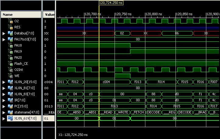
That was my problem!
Adding a D flip-flop to delay the RE by one cycle fixed it.
Thanks for pointing me in the right direction Arlet. Saved me at least a week, maybe 2!
1 thing I forgot to mention, hence this edit, is that XLXN_619[7:0] is the bus from the Flash MSB output ($C004) after the FD8CE (where the upper address is latched), after the Flash MUX's (which only pass data when RE is active), but before the OR gates to the 6502 DI. Sorry to try to explain schematics, but it isn't complete yet.
Before (incorrect):
After:
Now I'll use this technique for all the other RE's too, but I'll have to wait till "work" is over, before I head home and try it out!
EDIT: Explained XLXN_619[7:0] in the pics
Posted: Sun Apr 03, 2011 11:42 pm
by ElEctric_EyE
Just struck me on my 1hr drive home how to go about the next stage of fully interfacing with the Flash, while still taking advantage of the awesomeness of a 38MHz 6502. The idea goes back to my "on the fly" O2 clock switcher which started
here. I thought I had posted the schematic of the synchronizer I used...Here it is: the
original link for making clock switching glitch free.
Now
my new and improved idea is: instead of manually programming a speed bit in anticipation of accessing slow memory devices, whenever the slow
memory device is accessed, the O2 speed is auto switched to a frequency controlled by the address decoding. Will have to do some testing first.
Posted: Sat Apr 09, 2011 3:33 am
by ElEctric_EyE
I've now implemented the "clock switcher" circuit from my earlier project into this one. O2 (phase 2) to Arlet's 6502 core is either a 38.86MHz (from the DCM generating a 4:5 ratio from the original 48.58MHz out of the DS1085L), or a 12.14MHz (from the 48.58MHz DS1085L/4).
The address decoding signal to enable the Flash also controls the O2 speed. When the external 70ns Flash is selected, the same signal is used to select the O2 speed to slow the cpu core down to accomodate the slower data transfer.
So far it seems to be working. The Flash is consistently outputting all zero's at this point, although I was hoping for a more random pattern like SRAM's exhibit on power-up.
The software is looping and data is being written straight to the display. Incorrect data should easily be seen.
The only way to truly test my circuit at this point, is to "burn" this Flash with a pattern. Not a problem, although it will require more effort and time to follow the algorithm spec'd in the datasheet...
I'm thinking a FRAM would've been nice to use with similar access times and no special programming algorithms, but they are still small sizes I believe...
Posted: Sat Apr 09, 2011 7:25 am
by Arlet
All the flash chips I've seen contain all-ones data when they're new.
Posted: Sat Apr 09, 2011 6:21 pm
by Dr Jefyll
The address decoding signal to enable the Flash also controls the O2 speed. When the external 70ns Flash is selected, the same signal is used to select the O2 speed to slow the cpu core down to accomodate the slower data transfer.
It sounds as if your arrangement does more or less what RDY does in a conventional 65xx system. In both cases it's address decoding that provides the trigger; therefore the slowdown occurs automatically, and only during bus cycles which select a device which requires it. There
is a slight difference, of little or no consequence: RDY doesn't
prolong O2 (as you seem to be doing); it merely allows several O2's to elapse while the processor waits doing nothing. I notice Arlet's core, being quite succinct, doesn't feature a RDY input, so I guess your approach is a sensible alternative. Cheers,
Jeff
Posted: Sun Apr 10, 2011 1:14 pm
by ElEctric_EyE
You're right Arlet, checking the Flash's datasheet, when a chip erase is performed all '1's are written. Which means, I should be seeing a white screen, not a black one. I need to develop a timing scheme for off-chip databuses... Should have it sorted out soon.
Then plans are to add the PS2 core for the keyboard.
Thanks for stopping by Dr. Jeffyl. Your comments/help are always valued!
Posted: Mon Apr 11, 2011 12:53 am
by ElEctric_EyE
... RDY doesn't prolong O2 (as you seem to be doing); it merely allows several O2's to elapse while the processor waits doing nothing...
I think if I ran my system against yours, mine would be faster. Let me explain why...
You would "insert" wait state cycles by, hardware or software, while the cpu is running at top speed. This may be OK, but I think my idea is superior because it constantly runs at the max frequency of the CPU while also taking into account the min access time of the memory device, per the address decode. So if there where some different devices on the bus with different access times, the only problem is providing the max O2 frequency at any address decode.
Heh, I may regret this in the morning

Posted: Tue Apr 12, 2011 5:40 am
by Dr Jefyll
Heh, I may regret this in the morning
LOL!! Not sure what to make of this... and not sure whether or not I really want you to explain!

As for timing to accommodate slow memory, the topic is a little clumsy to discuss, so bear with me.
my idea [...] constantly runs at the max frequency of the CPU while also taking into account the min access time of the memory device, per the address decode.
Agreed. It's a good system you've come up with; it ensures the performance loss from using slow memory is no worse than absolutely necessary. But the quoted sentence
is also true of the RDY approach. RDY is pretty much the same as your approach. RDY uses slowdown circuitry that's mostly built into the CPU core, rather than added externally to the Clock generator. I wish I could offer a better explanation. It might be good to do some more reading on the subject and hear it explained in different words, or a schematic maybe.
-- Jeff
Posted: Tue Apr 12, 2011 6:05 am
by Arlet
Disadvantage of the clock switching method is that it needs to be done carefully to avoid glitches. It also creates extra delay in the clock path.
When I have some more time, I should take a look at what it takes to implement RDY in the core.