Page 10 of 20
Posted: Mon Nov 30, 2009 8:57 pm
by ElEctric_EyE
Did not have time today to investigate bitmaps yet....yet. I spent most of today aligning text and graphics. PITA. Next time I add two pots and 2 ADC's for X & Y adjustments, and a couple keys to make the intro screen much quicker.
The TPS reading is Throttle Position Sensor. 0%-100%.
Code: Select all
Broken external image link
http://i207.photobucket.com/albums/bb73/ultimateroadwarrior/DSCF0069.jpg
Posted: Tue Dec 01, 2009 2:01 pm
by ElEctric_EyE
I'm using a hex editor called HxD. It's free and does a good job... I've been looking at some simple 1 color 24 bit bitmap's I made in MS Paint. Converting them to 256 color bitmaps by using the "save as" function did not convert them from the 24 bit format to an 8 bit format as I thought it would. It seemed to just compress the data. When I looked at it in the hex editor, it had a bunch of odd numbers in no particular pattern. For Blue I found the pattern FF,00,00. For Red I found 00,00,FF. Process of elimination Green is 00,FF,00...
So for a first test I'll burn a small 24bit pic to the EEPROM and then the program will do the math to write it to the display. I'll truncate the lower? bits, do some ANDing and ADDing. I wish I could get into the pic aspect of the display but the amount of memory full pictures take are beyond the scope of this project. a 320x200x3 picture alone would be 192K. The 65816 processor with its 16MB of memory would be better suited I'm sure. But I would still like to do some 1-3K small icons (16x16 or 32x32).
In my previous post I guess I was asking if you guys knew of any hex editor that could do some simple math. At least truncation?
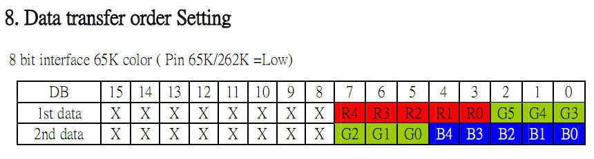
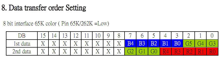
This is from the display datasheet. I think they have red and blue switched. Checking that right now...
Posted: Tue Dec 01, 2009 4:46 pm
by ElEctric_EyE
The red and blue IS switched. I know this because of the green data. The green is brightest when I send $07, $E0. Earlier, when I was having signal problems I would send $F0,$00 and get blue. But I knew data being sent was not 100% reliable, so I thought it was my circuit. Now that the signal problems are gone, I can confirm 100% the datasheet should look like this:
Posted: Mon Dec 07, 2009 4:54 pm
by ElEctric_EyE
NHD confirms the previous posts' correction...
Had some time today early on, to complete the software routine that "simulates" live data for the Air intake temp, coolant temp, and speed by incrementing a single register. This is the beginning of the "main loop". It displays enlarged 3 8 bit data being incremented from 0 to 255. The speed of the 6MHz 65C02 is quite impressive.
I'm going to make a very short video and post it on youtube (hopefully today), before I go on to make the routines for displaying the horizontal and vertical bar graph data. I expect these routines to slow the main loop down abit more. Displaying lines graphically may not slow it down as much as displaying enlarged characters though...
Anyway, just making the video to present the starting point for a speed reference. I plan on scrolling through all of the 2.2K worth of software as well. All suggestions/critiques are always most certainly welcome.
EDIT:330MB video is taking more than 4hours to upload... PITA
I edited my sig to include the link yesterday, but I guess it won't update until my next "fresh" post. Sorry for that.
Video link here:
http://www.youtube.com/watch?v=II4N6sLD ... re=channel
I know don't tell me, lay off the sauce.... My response: Tis' the season, heh, as long as I make progress...
Posted: Mon Feb 08, 2010 5:43 pm
by ElEctric_EyE
....I've been off making progress, learning, in the attempt to acquire more 65C02 speed. That thread can be read here:
viewtopic.php?t=1503 ...
Today's time has been spent updating pinouts. When I wirewrap, I like to follow a simple datasheet. Good luck on finding one for a CPLD. Many I/O options change the layout/# of pins. So first step for me was to make this pinout of the XC9572-10PCG44C, since I'll be using the same 44-pin PLCC socket that I used for the W65C02:
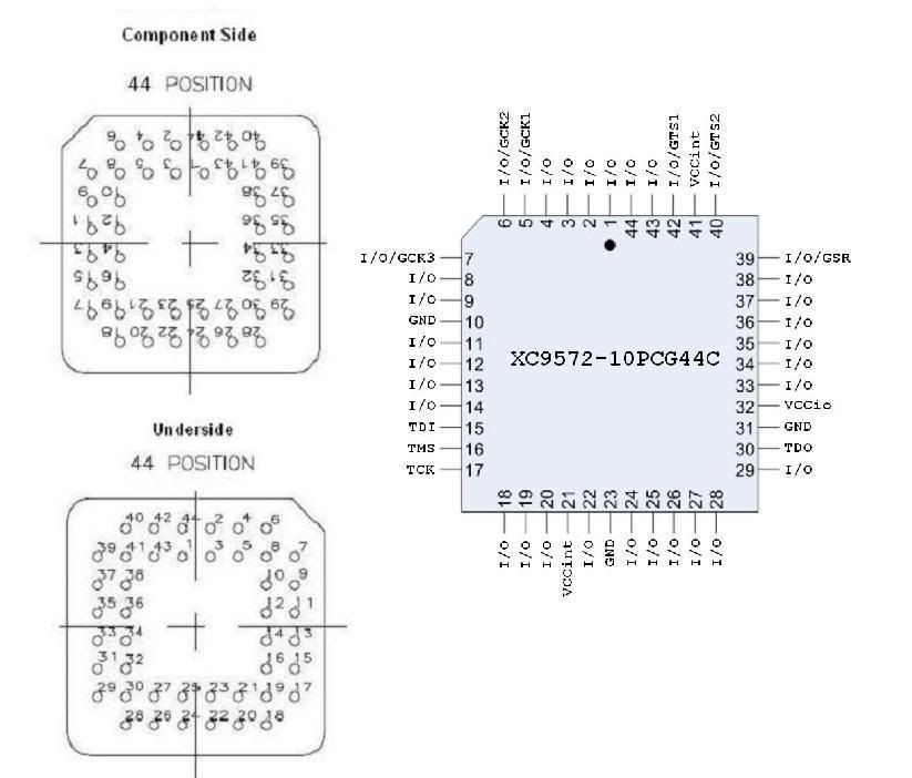
Keep in mind this family (XC95xxx) of Xylinx CPLD's is JTAG programmable, and has the dedicated pins. Time to wirewrap soon...
Posted: Mon Mar 08, 2010 6:18 pm
by ElEctric_EyE
I have not given up on this pulse width analyzer! By learning the Xilinx software to program the XC9572 for the address decoding/16K SRAM window in 512K data, I've learned the full capabilities of the CPLD. Next I wire up power and bypass cap's to the CPLD and the JTAG and see if I can program it. Then off to wiring the rest...
I'm using the same prototyping board, what's left on the real estate (8.5x8.5 .060" hole vector board), with a separate power connector to the next section.
Code: Select all
Broken external image link
http://i207.photobucket.com/albums/bb73/ultimateroadwarrior/CPLD1stmod.jpg
Posted: Thu Apr 01, 2010 10:06 pm
by ElEctric_EyE
Changed a few things... Found a new "hideout". Wife agreed to get my clutter out of the living room. I proposed a small corner of "our" room to fit in "my" project. So I set up a Pentium 3 slot 1 dedicated computer with all the software needed, and when noone is home, I continue my progress with zero distractions...
Just a few signals left to wire, which require switches, oscillators, etc. First wired up the power and bypass cap's, then data buses, then addresses, then chip selects/output enables, then "pull-up/downs", finally reset switches and oscillators. I've double and triple checked my wirewrap along the way. If any of you have done this you'll know when you're "obviously" wrong when you intend to wire a pin and it's already been wired. Then you've got to retrace who knows how far back... So far I've not run into it this time, in fact there were times I thought I was wrong, and to my relief after double and triple checking, found my wiring to be correct. (These are things wirewrappers understand, attention to detail from the schematic. Front side, reverse side, mirrored, where did I leave off, etc.). Anyway as usual, I thought I'd leave a couple pic's since it's so slow in here. I expect to power it up by Monday.
New workspace:
Code: Select all
Broken external image link
http://i207.photobucket.com/albums/bb73/ultimateroadwarrior/DSCF0110.jpg
Underneath:
Code: Select all
Broken external image link
http://i207.photobucket.com/albums/bb73/ultimateroadwarrior/DSCF0115.jpg
Posted: Fri Apr 02, 2010 10:28 am
by BigEd
I'm going to have to ask: what's this?
- heatsink.jpg (3.99 KiB) Viewed 4308 times
I can only suppose it's a heatsink. If it is, what's the hot chip underneath?
Posted: Fri Apr 02, 2010 11:49 am
by OwenS
Regarding the bitmap formats:
8-bit format generally means palletized, so the file contains an up to 256-entry palette of 24-bit colours, and the image data then indexes that. 16-bit generally means RGB data in 5:6:5 format, like your LCD. 24-bit means 3 bytes per pixel, but I'm sure you have figured that out by now

Posted: Sat Apr 03, 2010 1:06 am
by ElEctric_EyE
I'm going to have to ask: what's this?....
I can only suppose it's a heatsink. If it is, what's the hot chip underneath?
It is a heatsink on a 74S124 VCO good to 60MHz. I ran it @ around 20MHz, and the ****** got hot so I put one of my spare ramsinks ontop of it, just because of the heat generated by that "S" series chip, (you can't find it in another TTL family, just the "S" series.) I wasn't pushing it anywhere near the IC's limit BTW, but it still got quite hot, so I figured the cooler I kept it the more linear it would stay. I hate lack of thermal control, where it's needed...
Posted: Sun Apr 04, 2010 9:32 pm
by ElEctric_EyE
Regarding the bitmap formats:
8-bit format generally means palletized, so the file contains an up to 256-entry palette of 24-bit colours, and the image data then indexes that. 16-bit generally means RGB data in 5:6:5 format, like your LCD. 24-bit means 3 bytes per pixel, but I'm sure you have figured that out by now
Correct, this display has a few built in options, which you can set via jumpers on the back (I've had to mod one of the jumpers already to work in 68xx mode, I posted that awhile back). Currently my display is set for two consecutive 8 bit data in the 5-6-5 format (total 16 bits).
Well, I wired it all up, and the only thing working is reset. This is what happens when you try to skip a few building blocks along the way, I thought I was good. Obviously not good enough... However, this is my first attempt with CPLDs integrated right in the middle of a new design, controlling main clocks, and address decoding. And I have not touched the other circuit that has been working, so I have a reference to work from. Currently, the main clock is @10MHz, and when the initial part of the software is copying the 8K "OS" and 512K "data" EEPROMs to the SRAMs, the system is running @5MHz. Will have to break out the 'scope tomorrow and check the clock signals.
(P.S. I ordered the 55MHz 640x480 TFT display from Newhaven yesterday, so I have that on the backburner before experimenting with opcode mods, but that 5ns XC9536 is just waiting to be wired up after I master it's big brother)
Posted: Mon Apr 05, 2010 5:52 pm
by ElEctric_EyE
Checked the phase2 signals going into and out of the CPLD and they looked good and are switching from high and low speeds as expected.
Found a few problems with my design inside the CPLD. Working on it now. If any of you are curious, my software was doing an INC on the Bank register, which is only a flip-flop write to only. Trying to do CMP for the end of 512K window, it got stuck in an infinite loop since is was reading random data. I am programming in a latch, and tri-state buffer, and also wiring in a R/W signal.
Posted: Mon Apr 05, 2010 7:53 pm
by ElEctric_EyE
Here's a look inside the CPLD, pretty simple stuff:
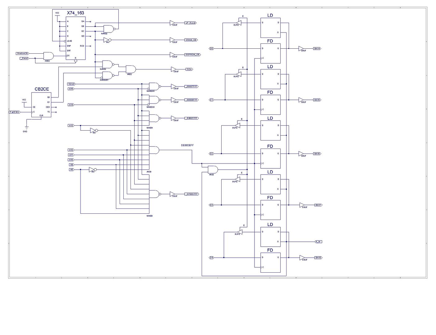
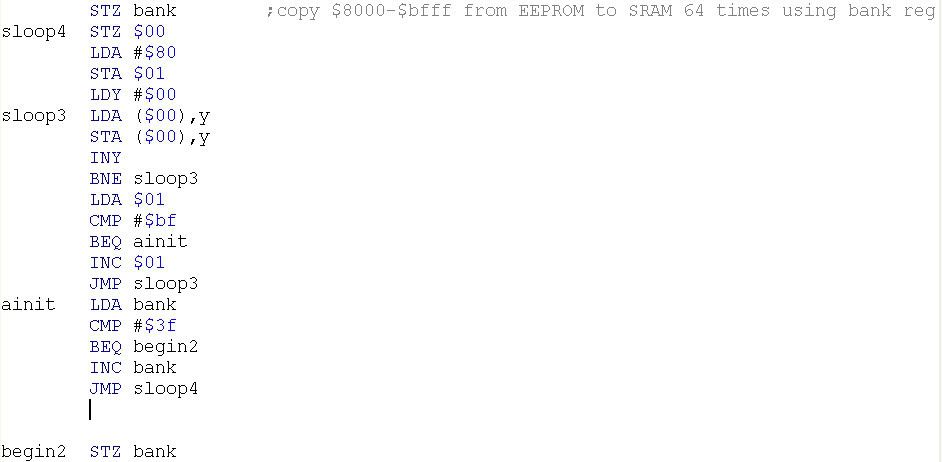
This is the software to copy the 512K EEPROM to 512 SRAM. Seems to be getting stuck here. If I comment out this part the program progresses... My mind is in hardware mode, maybe someone can help me out here. What am I missing? I'm sure it's software related...
Posted: Mon Apr 05, 2010 9:47 pm
by leeeeee
Have you tried with code that doesn't rely on being able to read the bank register?
This
should work.
Code: Select all
      LDY   #$00        ; clear the block index
      STY   $00         ; clear the pointer low byte
      LDX   #$00        ; clear the bank number
sloop4
      STX   bank        ; set the bank
      LDA   #$80
      STA   $01         ; reset the pointer high byte
sloop3
      LDA   ($00),Y     ; copy the byte ..
      STA   ($00),Y     ; .. to RAM
      INY
      BNE   sloop3      ; loop if more bytes to copy

      INC   $01
      LDA   $01
      CMP   #$C0        ; compare it with end + 1
      BNE   sloop3      ; loop if not there yet

      INX               ; increment the bank number
      CPX   #$40        ; compare it with end + 1
      BNE   sloop4      ; loop if not there yet

begin2
      STZ   bank
Lee.
Posted: Mon Apr 05, 2010 11:07 pm
by 8BIT
From the schematic, it looks like a write to DExx loads the upper address bytes. Is this the "bank" variable referenced in your code?
What address is this code being read from?
Is it possible that once you write the bank variable with a bank other than 0, (1 for example) that the program hangs because the PC now points to an address in bank 1 that does not contain valid program code?
Just a thought.
Daryl