6502.org Forum  Projects  Code  Documents  Tools  Forum
It is currently Sat Apr 20, 2024 1:59 pm

All times are UTC


Post new topic Reply to topic  [ 126 posts ]  Go to page Previous  1, 2, 3, 4, 5, 6, 7 ... 9  Next
Author Message
PostPosted: Fri Feb 04, 2022 7:45 pm 
Offline
User avatar

Joined: Sat Jul 24, 2021 1:37 pm
Posts: 282
Episode 16 is out!

In this episode, I re-work the address decoding circuit. I'm pretty happy with the result: Gone is the obsolete 74HC4078, which I was able to replace thanks to the 74AC563 inverting latch. I can now detect bank zero using a (N)AND gate rather than a (N)OR.

Here is the new circuit I came up with, and as you can see I still meet the propagation constraints for my 4MHz frequency goal.

Attachment:
address.png
address.png [ 342.59 KiB | Viewed 2545 times ]

_________________
BB816 Computer YouTube series


Top
 Profile  
Reply with quote  
PostPosted: Fri Feb 04, 2022 10:56 pm 
Offline

Joined: Sat Jul 31, 2021 4:57 am
Posts: 14
It’s neat to see test driven development of logic circuits, that’s a pretty good tool.


Top
 Profile  
Reply with quote  
PostPosted: Sat Feb 05, 2022 2:26 pm 
Offline
User avatar

Joined: Sat Jul 24, 2021 1:37 pm
Posts: 282
If you enjoy it and would like to see more I can recommend rj45's channel, he is building a CPU and a VDP from scratch in Digital: https://www.youtube.com/c/rj45Creates

_________________
BB816 Computer YouTube series


Top
 Profile  
Reply with quote  
PostPosted: Mon Feb 21, 2022 10:00 pm 
Offline
User avatar

Joined: Sat Jul 24, 2021 1:37 pm
Posts: 282
Episode 17 is out!

In this episode, I battle some signal integrity problems, as my memtest program is reporting bit flips on the data bus. I re-do my power delivery network and that seems to help a bit, but ultimately I think the length of my data bus and address bus wires is causing reflections, so the problem persists for now, albeit less frequent. Along the way, I add a Teensy bus monitor to help me see what's happening on the busses.

Hope you enjoy!

I'm considering moving to a backplane system, but I worry about how that is going to look on top-down video and how to integrate breadboard work on it. Looking at DIN 41612 connectors, or even PCIe x16 for better signal integrity (the former being specced up to 3MHz only apparently). I could go for PCIe cards, and use a PCIe ribbon extension to bring the signals to a breadboard?

Any feedback on this idea is welcome, as well as suggestions on how to fix my signal integrity problems on the current build

_________________
BB816 Computer YouTube series


Top
 Profile  
Reply with quote  
PostPosted: Tue Feb 22, 2022 3:40 pm 
Offline
User avatar

Joined: Fri Dec 11, 2009 3:50 pm
Posts: 3343
Location: Ontario, Canada
akohlbecker wrote:
suggestions on how to fix my signal integrity problems on the current build

It's best to avoid thinking of the Power & Ground Distribution network as something for connecting the chips to the power supply. Where high frequencies are concerned, its real job is to connect the chips to one another.

Imagine Chip A in Location A. We know it outputs a signal whose current gets carried by a conductor to Chip B, some distance away. It's easy to forget that, in order to complete the circuit, a return current must flow through the Power & Ground Distribution network from Chip B back to Chip A.

The return current will follow the path of least inductance (the resistance is low enough not to matter). Inductance is the enemy, and we can minimize inductance by providing a return path that's in close proximity to the signal path. This is crucial. The signal current and return current flow in opposite directions, and when two opposing currents are in close proximity their magnetic fields tend to mutually cancel. And that's what we want, because it reduces inductance.

(BTW there's another way of discussing this effect. Sometimes in reference documents the signal and return path are described as forming a loop, with the goal being to reduce the loop area -- and thus the number of lines of magnetic flux contained by the loop. Closer proximity means less loop area. In turn we get fewer lines of magnetic flux passing through the loop, which results in less inductance.)

The Power & Ground Distribution Network can support this by making many paths available. For every signal wire connecting Chip A to Chip B there would ideally also be, in close proximity to the signal wire, power and ground wires connecting Chip A and Chip B. This isn't practical on a wireless breadboard (or a 2-layer PCB), but you can achieve some of the same benefit by forming the Power & Ground Distribution network into a coarse grid (a fine grid is even better). Remember: the goal is that, for any signal from one chip to another, you want the return current to be able to follow much the same path, in close proximity, back to the first chip.

In the first diagram below I've highlighted your Power & Ground Distribution network, and we can see that, as a grid, it has many serious gaps. If this were the roadmap of a city we'd say it has far too many cul de sacs, making driving a nightmare. The second diagram shows some possible connections you could add to provide relief to the frustrated drivers!
Attachment:
'as is'.png
'as is'.png [ 661.41 KiB | Viewed 2442 times ]
Attachment:
improved grid.png
improved grid.png [ 425.67 KiB | Viewed 2442 times ]


And, here's another diagram suggesting a further improvement. Since you have several bundles of conductors in midair, vertically separated from the grid, you would do well to add at least a ground wire in close proximity to each of those bundles. Because the goal is to conduct current, both end points (not just one) need to attach to the local ground. (And if there are three or more end points, all should ideally be grounded.)
Attachment:
specific return paths.png
specific return paths.png [ 423.93 KiB | Viewed 2442 times ]


Hope this helps. I think we could also improve the way your bypass capacitors are arranged, but that's a topic for another post.

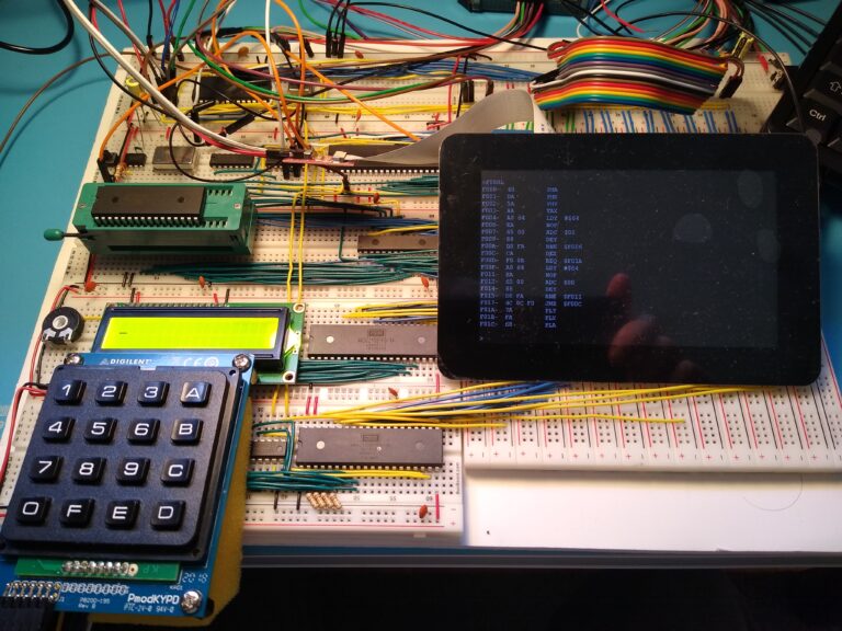
The WDC '816 is always challenge, due to the very fast transitions on its outputs. And with a breadboard project of this size you may only find it possible to reduce the number of glitches, rather than eliminating them entirely. :|

BTW you may also want to see my recent post here, also on the subject of Power & Ground Distribution grids.

-- Jeff

_________________
In 1988 my 65C02 got six new registers and 44 new full-speed instructions!
https://laughtonelectronics.com/Arcana/ ... mmary.html


Last edited by Dr Jefyll on Tue Feb 22, 2022 7:09 pm, edited 1 time in total.

Top
 Profile  
Reply with quote  
PostPosted: Tue Feb 22, 2022 6:56 pm 
Offline

Joined: Fri Dec 21, 2018 1:05 am
Posts: 1076
Location: Albuquerque NM USA
Dr Jefyll wrote:
It's best to avoid thinking of the Power & Ground Distribution network as something for connecting the chips to the power supply. Where high frequencies are concerned, its real job is to connect the chips to one another.

Let me enthusiastically echo Dr. J's comment above. I sacrificed one Christmas Holiday in 1990's trouble-shooting the "tuning fork" power distribution shown in the "as is" picture. I had a board with similar power/ground distribution configuration with octal tranceivers pair located at the ends of the "tuning fork", one at each arm. They communicated to each other flawlessly for many years until we replaced the 54LS245 with the fast IDT54FCT245 buffers. Then it failed intermittently inside temperature chamber (low temperature, high voltage when 54FCT245 is fastest). Ultimately it was because when multiple signals are switching simultaneously, the ground of one arm was rising (due to inductance) above the switching threshold of the other arm causing faulty data to be written or read. It doesn't matter how well each arm was bypassed. The fix was to tie the end of the tuning fork distribution into grid just like Dr. J's "improved grid" picture. My one sentence summary of that experience was "It doesn't matter how powerful Superman is (54FCT245 was like Superman compare to 54LS245), he can't lift a building if the ground he stands on is soft mud!"
Bill


Top
 Profile  
Reply with quote  
PostPosted: Tue Feb 22, 2022 9:55 pm 
Offline
User avatar

Joined: Sat Jul 24, 2021 1:37 pm
Posts: 282
Thank you both for the great information! And even with pictures!

I've been avoiding making those ground connections for fear of creating ground loops. I guess I need to reconsider that :-)

_________________
BB816 Computer YouTube series


Top
 Profile  
Reply with quote  
PostPosted: Sun Feb 27, 2022 8:27 pm 
Offline

Joined: Sat Feb 19, 2022 10:14 pm
Posts: 147
akohlbecker wrote:
... I think the length of my data bus and address bus wires is causing reflections ...


I had similar problems when trying to run a testbed 6502 build with long address and data buses at higher clock speeds.

Image

That prompted me to make a speed test build as compact as possible.

Image

I could only operate the build with longer buses at 2 MHz but the more compact one at 10 MHz.

btw: great video series. I've learned a lot and hope to incorporate some of your ideas into my 65816 build.


Top
 Profile  
Reply with quote  
PostPosted: Sun Feb 27, 2022 10:08 pm 
Offline
User avatar

Joined: Fri Dec 11, 2009 3:50 pm
Posts: 3343
Location: Ontario, Canada
Just a little hint, tmr4. On this forum you're allowed to attach images with your posts. You'll find this more convenient than hosting images off-site, and furthermore the images will remain available long-term for future readers of the forum. Cheers,

Jeff

_________________
In 1988 my 65C02 got six new registers and 44 new full-speed instructions!
https://laughtonelectronics.com/Arcana/ ... mmary.html


Top
 Profile  
Reply with quote  
PostPosted: Sun Feb 27, 2022 10:37 pm 
Offline
User avatar

Joined: Sat Jul 24, 2021 1:37 pm
Posts: 282
tmr4 wrote:
btw: great video series. I've learned a lot and hope to incorporate some of your ideas into my 65816 build.


Thank you!

And thanks for sharing your build. The difference in speed is massive indeed.

_________________
BB816 Computer YouTube series


Top
 Profile  
Reply with quote  
PostPosted: Sun Feb 27, 2022 10:39 pm 
Offline
User avatar

Joined: Sat Jul 24, 2021 1:37 pm
Posts: 282
Also, I didn't post the regular video update yet! Episode 18 is out!

In that episode, I discuss the purpose of the VDA and VPA pins. I then add them to my debug LEDs and to my Arduino monitor.
I also start re-working my read-write pulses, to incorporate VDA/VPA and also RDY and BE. This leads to some interesting timing problems, which I'm hoping to solve next time with a new clock phase

_________________
BB816 Computer YouTube series


Top
 Profile  
Reply with quote  
PostPosted: Mon Feb 28, 2022 4:49 pm 
Offline

Joined: Sat Feb 19, 2022 10:14 pm
Posts: 147
Dr Jefyll wrote:
Just a little hint, tmr4. On this forum you're allowed to attach images with your posts...


Ah. Thanks. I was looking for that option in the style button area but didn't notice it was further down the page.


Top
 Profile  
Reply with quote  
PostPosted: Sun Mar 06, 2022 4:54 pm 
Offline
User avatar

Joined: Tue Aug 11, 2020 3:45 am
Posts: 311
Location: A magnetic field
As noted by Dr Jefyll, you've got fans and followers. However, they are copying some of your more exploratory steps without success.

I'm glad that you dumped the 74HC4078. I bought one to settle an argument with the argumentative BigDumbDinosaur. However, when I had it in my hoof (see username), I realized that it wasn't necessary. Instead, I devised a much faster scheme which treats all banks symmetrically. (Diagrams.)

akohlbecker on Tue 22 Feb 2022 wrote:
fear of creating ground loops.


Low frequency audio and a ground loop with large area should be avoided. High frequency digital and a ground loop with small area is highly desirable.

Tangentially related: Metal film resistors are usually best for low frequency audio and carbon resistors are usually best for high frequency digital. This is due to high inductance of metal film resistors and hiss from carbon resistors.

General principle: Electronics advice may not apply to your domain.

_________________
Modules | Processors | Boards | Boxes | Beep, Beep! I'm a sheep!


Top
 Profile  
Reply with quote  
PostPosted: Sun Mar 06, 2022 9:43 pm 
Offline
User avatar

Joined: Fri Aug 30, 2002 1:09 am
Posts: 8425
Location: Southern California
Sheep64 wrote:
Tangentially related: Metal film resistors are usually best for low frequency audio and carbon resistors are usually best for high frequency digital. This is due to high inductance of metal film resistors and hiss from carbon resistors.

Carbon-film thru-hole resistors have a spiral laser-cut in them to trim to the right value, and this spiral adds inductance; but the inductive reactance at the speeds we deal with here will usually be low compared to the resistance of the resistor. There's also the inductance of the body and leads which would be there even if there were no spiral cut in the carbon that coats the ceramic slug. Carbon-composition resistor OTOH have no spiral (and their tolerance is poor also compared to that of carbon-film resistors). Chip resistors are laser-trimmed from just one side of the tiny carbon rectangle, so there's no spiral cut in them. Their small body and lack of leads also reduces inductance. But yes, in the 1970's and 80's when I made my own audiophile equipment, I liked to use metal-film resistors for low noise.

_________________
http://WilsonMinesCo.com/ lots of 6502 resources
The "second front page" is http://wilsonminesco.com/links.html .
What's an additional VIA among friends, anyhow?


Top
 Profile  
Reply with quote  
PostPosted: Sun Mar 06, 2022 11:14 pm 
Offline
User avatar

Joined: Thu May 28, 2009 9:46 pm
Posts: 8138
Location: Midwestern USA
Sheep64 wrote:
Tangentially related: Metal film resistors are usually best for low frequency audio and carbon resistors are usually best for high frequency digital.

Technically, that is true, but some pink noise (aka hiss) is part and parcel of the vacuum tube audio amplifier era, no matter the resistor type (carbon comp in those days). Most of the hiss was thermionic noise being emitted by the tubes, especially in the early stages of amplification. Add to that the hiss generated by analog magnetic tape, along with a smattering of power supply ripple and traces of common mode hum, and you have what passed for “high fidelity” back when Eisenhower was the US president. My old Ampeg B15N bass amp has similar characteristics, just louder than what I had when I was in eighth grade, when a 20 watt amp was a real powerhouse. :D

As Garth noted, the tiny bit of inductance introduced by the spiral trim of a film resistor is usually of little-to-no consequence—lead lengths and general construction techniques will have more influence in most cases.

_________________
x86?  We ain't got no x86.  We don't NEED no stinking x86!


Top
 Profile  
Reply with quote  
Display posts from previous:  Sort by  
Post new topic Reply to topic  [ 126 posts ]  Go to page Previous  1, 2, 3, 4, 5, 6, 7 ... 9  Next

All times are UTC


Who is online

Users browsing this forum: Google [Bot] and 1 guest


You cannot post new topics in this forum
You cannot reply to topics in this forum
You cannot edit your posts in this forum
You cannot delete your posts in this forum
You cannot post attachments in this forum

Search for:
Jump to: