Hi there-- I'm writing an article for my engineering blog, and one section of it is on the 6502.
Does anyone know if there is reliable information about the process geometry of the original 6502 from 1975? Wikipedia mentions 8 micron, but the source is a brief note on a Sun Microsystems webpage by someone peripherally involved in the 6502 effort and it seems somewhat sketchy to me.
Alternatively, if there are any die shots out there of the original 6502, is it possible to determine geometry from the images and the full die size?
Process geometry information of original 1975 MOS 6502
-
jms_embedded
- Posts: 9
- Joined: 04 Jan 2022
Re: Process geometry information of original 1975 MOS 6502
Welcome! Yes, the various microphotographs of original 6502 die will tell you something about the process size.
Previous calculations suggest 5 micron for the 6502 captured for the visual6502 project.
Segher has said:From that, i get a north-south dimension of 3.5mm; and that leads
to a minimum gate length of 4.75um, so maybe it is 5um? I thought
it was supposed to be 8um. I get metal track pitch of 17.5um fwiw.
and Peter Monta replied:
(The track pitch of 17.5u might well imply a metal width of 8u, which someone might have taken to be the process node. But the transistor gate length, usually as the as-drawn width of polysilicon, was the usual measure in my day.)
Previous calculations suggest 5 micron for the 6502 captured for the visual6502 project.
Segher has said:
Quote:
Quote:
There's a good image of the die still in the package on slide 20 of 65
http://visual6502.org/docs/6502_in_action_14_web.pdf
http://visual6502.org/docs/6502_in_action_14_web.pdf
to a minimum gate length of 4.75um, so maybe it is 5um? I thought
it was supposed to be 8um. I get metal track pitch of 17.5um fwiw.
Quote:
Yes, I get pretty much the same numbers: overall chip size of 3.7 by 3.3 mm
(12 square millimeters) and about 5 micron transistors.
(12 square millimeters) and about 5 micron transistors.
-
jms_embedded
- Posts: 9
- Joined: 04 Jan 2022
Re: Process geometry information of original 1975 MOS 6502
Thanks for the reply!
Oh, that's interesting! So the issue here is that the version of the 6502 used on visual6502.org is revision D. (see slide 24 as well as http://www.visual6502.org/images/6502/index.html)
The original 1975 chip (rev A? not sure) was 168 x 183 mils (=4.27mm x 4.65 mm), according to EDN's article in September 1975, which mentioned that it "will be shrunk 10% to 153x168 mils soon". (=3.89mm x 4.27mm)
I can't remember exactly where I read it, but I seem to remember that the 10% shrink was an engineering design improvement rather than a process change. (I will edit this comment if I find the source again)
At any rate, I wouldn't be surprised if the rev D used in visual6502.org was 5um.
Just to crunch some ratios assuming a pure die shrink without any redesign: (4.27 mm x 3.89 mm of the 10% die shrink mentioned in EDN)/(3.7mm x 3.3mm mentioned in your quoted excerpt) = something in the 1.15 - 1.18 range, which would more likely imply that the original 6502 was around 6um rather than 8um. But that's just me with a quick off-the-cuff extrapolation.
I really wish the people who take the time to create these amazing die shots would include a reference gauge in their photos so it is possible to determine the die size. (and document which date code they used)
Pauli Rautakorpi aka birdman86 has a ton of die shots on Wikipedia (does anyone have his contact information?) including a Rev A 6502 but what are the exact die dimensions? ¯\_(ツ)_/¯
BigEd wrote:
Welcome! Yes, the various microphotographs of original 6502 die will tell you something about the process size.
Previous calculations suggest 5 micron for the 6502 captured for the visual6502 project.
Segher has said:From that, i get a north-south dimension of 3.5mm; and that leads
to a minimum gate length of 4.75um, so maybe it is 5um? I thought
it was supposed to be 8um. I get metal track pitch of 17.5um fwiw.
and Peter Monta replied:
(The track pitch of 17.5u might well imply a metal width of 8u, which someone might have taken to be the process node. But the transistor gate length, usually as the as-drawn width of polysilicon, was the usual measure in my day.)
Previous calculations suggest 5 micron for the 6502 captured for the visual6502 project.
Segher has said:
Quote:
Quote:
There's a good image of the die still in the package on slide 20 of 65
http://visual6502.org/docs/6502_in_action_14_web.pdf
http://visual6502.org/docs/6502_in_action_14_web.pdf
to a minimum gate length of 4.75um, so maybe it is 5um? I thought
it was supposed to be 8um. I get metal track pitch of 17.5um fwiw.
Quote:
Yes, I get pretty much the same numbers: overall chip size of 3.7 by 3.3 mm
(12 square millimeters) and about 5 micron transistors.
(12 square millimeters) and about 5 micron transistors.
The original 1975 chip (rev A? not sure) was 168 x 183 mils (=4.27mm x 4.65 mm), according to EDN's article in September 1975, which mentioned that it "will be shrunk 10% to 153x168 mils soon". (=3.89mm x 4.27mm)
I can't remember exactly where I read it, but I seem to remember that the 10% shrink was an engineering design improvement rather than a process change. (I will edit this comment if I find the source again)
At any rate, I wouldn't be surprised if the rev D used in visual6502.org was 5um.
Just to crunch some ratios assuming a pure die shrink without any redesign: (4.27 mm x 3.89 mm of the 10% die shrink mentioned in EDN)/(3.7mm x 3.3mm mentioned in your quoted excerpt) = something in the 1.15 - 1.18 range, which would more likely imply that the original 6502 was around 6um rather than 8um. But that's just me with a quick off-the-cuff extrapolation.
I really wish the people who take the time to create these amazing die shots would include a reference gauge in their photos
Pauli Rautakorpi aka birdman86 has a ton of die shots on Wikipedia (does anyone have his contact information?) including a Rev A 6502 but what are the exact die dimensions? ¯\_(ツ)_/¯
Re: Process geometry information of original 1975 MOS 6502
Oh, well spotted. I must have read that EDN article many times but have not remembered the planned shrink.
You'll note, then, that the rev D is a more dramatic shrink than 10%. Possibly there was only one shrink, or just possibly more than one. The preference for this sort of thing is a pure optical shrink - there is no new design work and no new layout. A conservative circuit design without too many analogue tricks is a better starting point in this case. The benefit of an optical shrink is that it's quicker and cheaper to try it, and it's purely a process problem to get it working, which means no to-and-fro between the process people, the layout people and the electronics people.
Eventually, process shrinks regularised at about 1.4x, such that the die area of a dense product like a RAM will halve each time. But in the early 70s, with an in-house fab, anything goes. Even a 10% linear shrink is a 20% area shrink, which as it turns out is better than a 20% cost reduction. And MOS's primary goal was to make the 6502 much cheaper than the competition.
In reality, the logic or circuit changes from Rev A to Rev D will necessarily have meant a need for layout changes - not necessarily for all layers - and therefore updated masks. One of MOS's innovations was direct tweaking of masks without remaking them - this was intended to fix mask defects but could possibly have allowed for minor layout changes too. Again, that would be cheaper and possibly faster than making a new mask.
So, the circuit revisions can, in some cases, proceed independently of moderate process shrinks, especially in those early days.
As you say, the ratios of measurements might support the hypothesis of a shrink from a 6u to a 5u process.
Re: Process geometry information of original 1975 MOS 6502
Having said all that, I see from the positions of the pads around the periphery that the rev A and rev D are different layouts. Even in thumbnails we can see this
- on the left, rev A has a single pad inboard of the chip edge, whereas rev D has two pads inboard.
- on the right, rev A has 8 bonded pads at the bottom, and a single pad at the top, whereas rev D has 7 pads bonded at the bottom and 2 at the top.
- on the left, rev A has a single pad inboard of the chip edge, whereas rev D has two pads inboard.
- on the right, rev A has 8 bonded pads at the bottom, and a single pad at the top, whereas rev D has 7 pads bonded at the bottom and 2 at the top.
-
jms_embedded
- Posts: 9
- Joined: 04 Jan 2022
Re: Process geometry information of original 1975 MOS 6502
fyi Visual6502's slide presentation shows a plastic chip labeled "MOS 6502 1683" = 16th week of 1983. Not sure if that is a rev D. (I wish they'd documented which chip they used a little more carefully!)
Walt Eisenhower's resume on team6502.org says:
I could swear I remember reading something else about the initial die shrink of the 6502, but can't find it at the moment.
Walt Eisenhower's resume on team6502.org says:
Quote:
Oct. 1979 to present - MOS Technology, Inc. Manager, Advanced Process Development
Developed production techniques for NMOS Product line making nearly 10,000 starts per week of 4" using 5 micron rules. Presently phasing-in 4 micron process and developing 3.5 process - utilizing latest technology - plasma etching, and deposition, cassette-to-cassette sputtering, etc. Consultant to sister division bringing 5" line on stream
Developed production techniques for NMOS Product line making nearly 10,000 starts per week of 4" using 5 micron rules. Presently phasing-in 4 micron process and developing 3.5 process - utilizing latest technology - plasma etching, and deposition, cassette-to-cassette sputtering, etc. Consultant to sister division bringing 5" line on stream
-
jms_embedded
- Posts: 9
- Joined: 04 Jan 2022
Re: Process geometry information of original 1975 MOS 6502
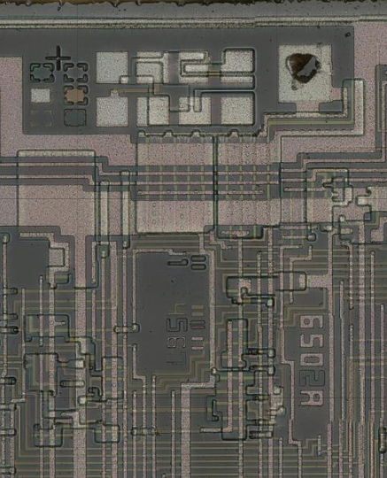
BTW Antoine Bercovici (@siliconinsid) posted a hi-res photomicrograph of a white-package 6502 rev A a few months ago on https://siliconpr0n.org/archive/doku.ph ... :mos:6502a (interactive viewer at https://siliconpr0n.org/map/mos/6502a/mz/, twitter announcement: https://twitter.com/siliconinsid/status ... 6901727236)
excerpt:

excerpt:

Re: Process geometry information of original 1975 MOS 6502
Oh, very nice indeed! If we knew the exact die size we could work out the approximate gate length (aka poly width)
-
jms_embedded
- Posts: 9
- Joined: 04 Jan 2022
Re: Process geometry information of original 1975 MOS 6502
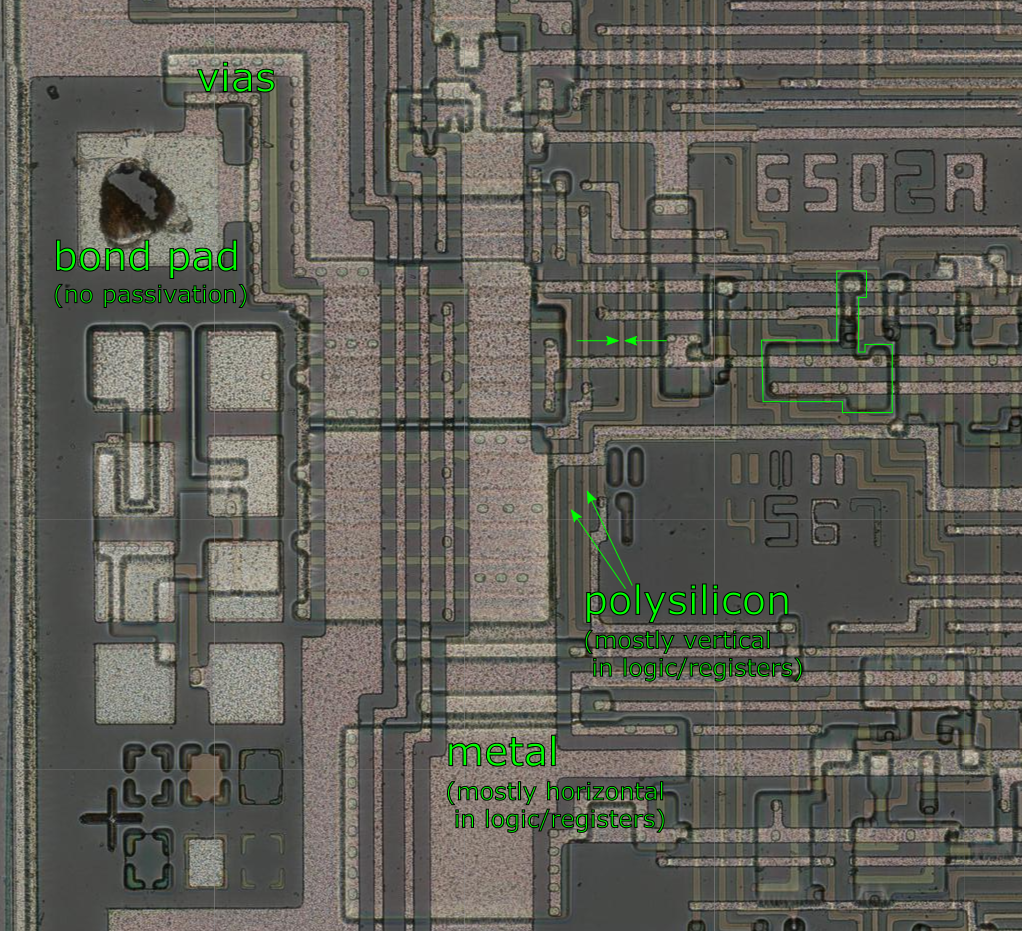
Just so I get the photomicrograph interpretation right, here's an annotated image of that area (rotated the "right way" with decode ROM PLA at top, control logic in middle, registers at bottom, text right side up)

Odd that they would draw 650_A in metal and then the 2 in mask 5 to show which variant; I would have expected the variant digit to show up in metal, to keep the lower-level masks the same.

- the funny submarine-with-periscope shape (outlined in green) is an example of a region with diffusion layer
- metal layer is pinkish speckled, except where it's exposed as contacts (not covered with a passivation layer) as in the bond pads, in which case it's grayish speckled; metal is mostly horizontal in the control logic/register sections
- polysilicon layer is brownish lines mostly vertical in the control logic/register sections
- vias are the little oval dots that are sometimes visible
- the green arrows pointing toward a polysilicon track would be the place to measure gate length = poly width
- mask 1 = diffusion
- mask 2 (not visible) = ? the grayish stuff?
- mask 3 (faintly visible) = ?
- mask 4 = polysilicon
- mask 5 = ?
- mask 6 = metal
- mask 7 = passivation
Odd that they would draw 650_A in metal and then the 2 in mask 5 to show which variant; I would have expected the variant digit to show up in metal, to keep the lower-level masks the same.
Last edited by jms_embedded on Sun Jan 09, 2022 9:44 pm, edited 1 time in total.
Re: Process geometry information of original 1975 MOS 6502
Sounds about right to me. Just one terminological thing: I've always seen contacts down to poly or diffusion described as contacts or contact cuts. Vias, in my world, are cuts between one metal layer and another, and of course there are none in a single-metal process like this. (Sometimes vias are not just a cut, but a conductive pillar through the oxide.)
About the green arrows: yes and no. The tracks in that area look a bit thin. This might be an optical effect, or a real one. The thing to measure would be the poly as it crosses diffusion, which makes a transistor - see the three of those going north to south over the "submarine" - they look a bit wider to me.
(Also to note, sometimes you will see diffusion labelled as active area - same thing, different terminology.)
Oh, another thing, the cuts in the passivation layer, that's mask 7, I wouldn't call that a contact. Sometimes passivation will be called overglass, in another variation of terminology.)
Oh, also, probably better to call the 7 numbered things masks, rather than layers.
-
jms_embedded
- Posts: 9
- Joined: 04 Jan 2022
Re: Process geometry information of original 1975 MOS 6502
Quote:
Oh, also, probably better to call the 7 numbered things masks, rather than layers.
I tried measuring in 6 places and got the following poly widths (through my crude eyeballing method), where "nm" is whatever scaling factor is applied on the image. The whole die is about 39550 x 43840 "nm" (39550 = east-to-west aligned with text, which is up-down in the existing image)
# https://siliconpr0n.org/map/mos/6502a/m ... =14809&z=8
# 61nm
# https://siliconpr0n.org/map/mos/6502a/m ... =15352&z=8
# 62nm
# https://siliconpr0n.org/map/mos/6502a/m ... =14789&z=8
# 59nm
# https://siliconpr0n.org/map/mos/6502a/m ... y=8144&z=8
# 67nm
# https://siliconpr0n.org/map/mos/6502a/m ... y=8171&z=8
# 71nm
# https://siliconpr0n.org/map/mos/6502a/m ... y=6184&z=8
# 65nm
Throwing away the high and low, I get an average of 64nm = approx 0.162% of full die width.
For a real die of 168 x 183 mils (=4.27mm x 4.65 mm) (quoting EDN article) this would mean a poly width of 6.9um.
For a real die of 153 x 168 mils (=3.89mm x 4.27mm), this would mean a poly width of 6.3um.
Not sure what to make of that; I'll see what @Siliconinsid comes back with, for the full die size.