This is the second entry pertinent to this thread: viewtopic.php?f=1&t=6777
So I had some time, and I implemented a design using this, from BigDumbDinosaur, for decoding read and write: viewtopic.php?f=1&t=6777#p87016
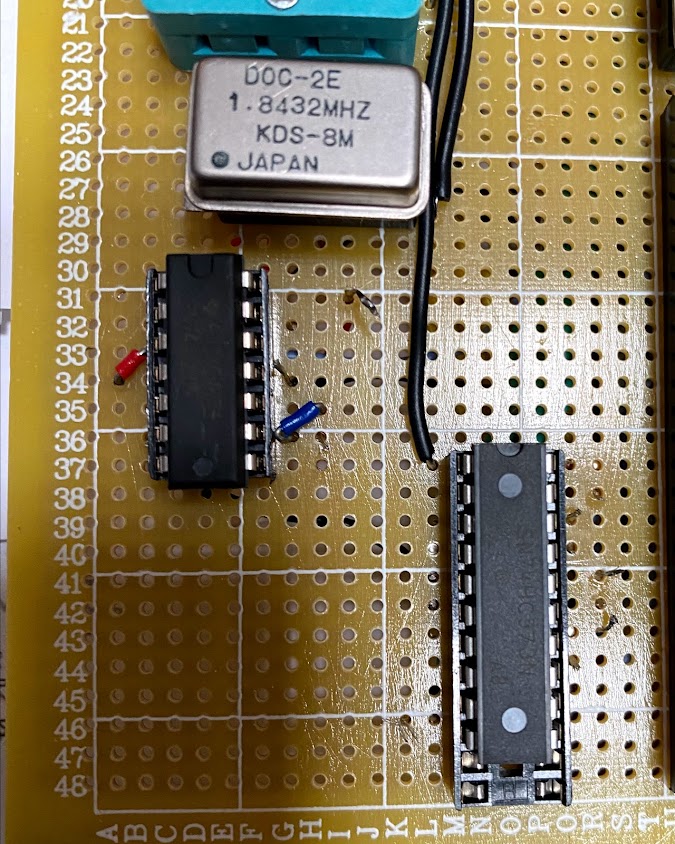
I implemented this in one 74AC00.
https://photos.google.com/u/2/share/AF1 ... RMZmxFOERn
I used Dr. Jefyll's connection scheme: viewtopic.php?f=1&t=6777#p87025
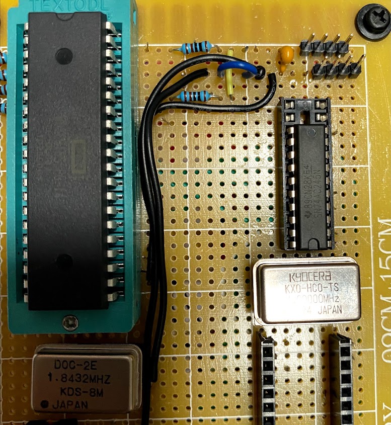
It goes through a 74AC245: https://photos.google.com/u/2/share/AF1 ... RMZmxFOERn
As you guys said, the B side faces the CPU and the A side faces outward to the bus.
Then, I implemented the bank address capture scheme found in the 65c816 data sheet, through a 74HC573: https://photos.google.com/u/2/share/AF1 ... RMZmxFOERn
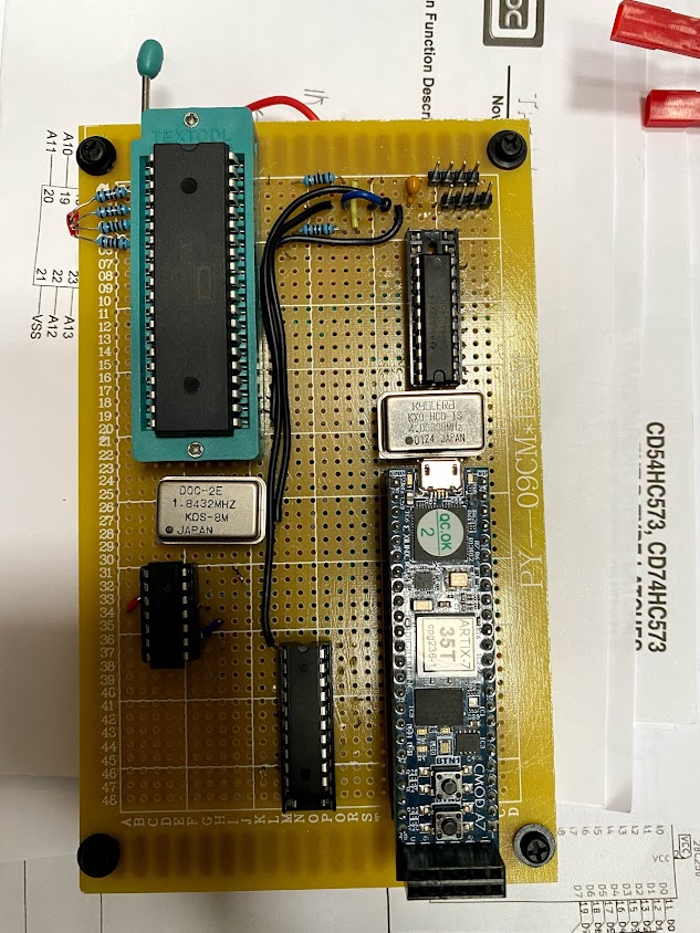
Then I ran all the lines (data out from the '245, bank addresses from the '573, addresses from the cpu, and /rd and /wr from the '00) into a CMOD A7 35T (has 512k SRAM): https://photos.google.com/u/2/share/AF1 ... RMZmxFOERn
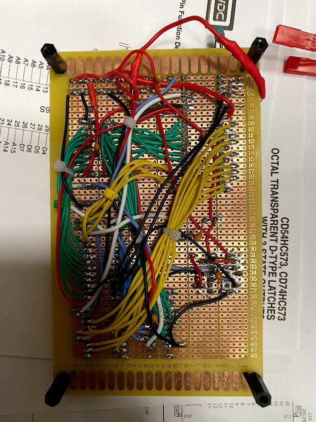
I was extremely careful with the wiring, testing and retesting with the multimeter as a soldered. I also ran a 4mhz clock into the FPGA for phi2 and a 1.8432mhz into the FPGA for LIV2's soft ACIA.
I tested extensively with my multimeter and logic probe, and I caught one issue, but everything checks out now.
My usual verilog tricks don't seem to work. Even with all those signals generated in hardware, I cannot get it to play nice. Can someone propose a verilog scheme that might work? I'm just trying to hook the cpu signals into the internal SRAM and LIV2's acia for basic testing and verification.
I have the data signals from Port A of the '245.
I have the bank signals from the '573.
I have all the processor signals.
And I have the /rd and /wr from the '00.
Jonathan
PS The specs for the CMOD A7 35T can be found here: https://digilent.com/reference/programm ... d-a7/start
Simple Question: 65c816 - Part Deux!
Simple Question: 65c816 - Part Deux!
Last edited by Jmstein7 on Fri Sep 17, 2021 4:50 pm, edited 3 times in total.
Re: Simple Question: 65c816 - Part Deux!
Here are the images:

Re: Simple Question: 65c816 - Part Deux!
First comment I think is that you don't have enough decoupling capacitance. Normally we see one electrolytic where the power is brought to the board, and then a ceramic or tantalum next to each chip.
Next, you need to know that you've built what you've designed. So, with all chips out, and your multimeter in continuity mode, you need to test all the pin-pairs which should be connected, to check that they are connected, and then test all pins against the adjacent pin, to check that they are not shorted (unless they are supposed to be.) This only takes a few seconds per pin.
And then, I think you're looking for a review of what you've designed.
After fixing up the capacitors and performing the circuit checks, put your chips back in, and tell us what you see and what you don't see.
Re: Simple Question: 65c816 - Part Deux!
BigEd wrote:
First comment I think is that you don't have enough decoupling capacitance. Normally we see one electrolytic where the power is brought to the board, and then a ceramic or tantalum next to each chip.
Next, you need to know that you've built what you've designed. So, with all chips out, and your multimeter in continuity mode, you need to test all the pin-pairs which should be connected, to check that they are connected, and then test all pins against the adjacent pin, to check that they are not shorted (unless they are supposed to be.) This only takes a few seconds per pin.
And then, I think you're looking for a review of what you've designed.
After fixing up the capacitors and performing the circuit checks, put your chips back in, and tell us what you see and what you don't see.
Next, you need to know that you've built what you've designed. So, with all chips out, and your multimeter in continuity mode, you need to test all the pin-pairs which should be connected, to check that they are connected, and then test all pins against the adjacent pin, to check that they are not shorted (unless they are supposed to be.) This only takes a few seconds per pin.
And then, I think you're looking for a review of what you've designed.
After fixing up the capacitors and performing the circuit checks, put your chips back in, and tell us what you see and what you don't see.
PS do the resistors on the cpu look properly placed?
Re: Simple Question: 65c816 - Part Deux!
Good news on the caps.
I notice your 245 is upside down compared to the other chips. That may be as intended, but as a principle of least surprise it's worth placing all chips the same way up.
I notice your 245 is upside down compared to the other chips. That may be as intended, but as a principle of least surprise it's worth placing all chips the same way up.
Re: Simple Question: 65c816 - Part Deux!
BigEd wrote:
Good news on the caps.
I notice your 245 is upside down compared to the other chips. That may be as intended, but as a principle of least surprise it's worth placing all chips the same way up.
I notice your 245 is upside down compared to the other chips. That may be as intended, but as a principle of least surprise it's worth placing all chips the same way up.

Re: Simple Question: 65c816 - Part Deux!
You could use the integrated logic analyzer (ILA) component to dump the signals as the FPGA sees them.
This would show if the address / data is what is expected.
Is block RAM in the FPGA being used as the ROM?
This would show if the address / data is what is expected.
Is block RAM in the FPGA being used as the ROM?
Re: Simple Question: 65c816 - Part Deux!
Rob Finch wrote:
You could use the integrated logic analyzer (ILA) component to dump the signals as the FPGA sees them.
This would show if the address / data is what is expected.
Is block RAM in the FPGA being used as the ROM?
This would show if the address / data is what is expected.
Is block RAM in the FPGA being used as the ROM?
Anyway, no, I'm using distributed memory, not block. I'm trying to keep everything asynchronous, as much as possible, to match the operation of the 'c816 bus.
I'm using a VIO and single-stepping to test. I don't know how to use the ILA IP core.
Jon
Re: Simple Question: 65c816 - Part Deux!
Oh, I probably should have posted this earlier - my code! 
Here it is: https://github.com/jmstein7/65c02-FPGA- ... bench.srcs
Sorry!
Jon
Edit: to switch from run mode to diagnostic mode, comment-out the clock module and comment-in the VIO. Do the reverse to go back to run mode. In diagnostic mode, phi2 toggles the clock signal.
Here it is: https://github.com/jmstein7/65c02-FPGA- ... bench.srcs
Sorry!
Jon
Edit: to switch from run mode to diagnostic mode, comment-out the clock module and comment-in the VIO. Do the reverse to go back to run mode. In diagnostic mode, phi2 toggles the clock signal.