Hi people,
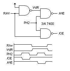
Browsing around this site (and the projects linked off it), I have seen two ways of generating Intel like /RD and /WR strobes the most common seems to consist of 3 NAND gates that generate /RD and /WR such that
/RD = R/W NAND PHI2
/WR = (NOT R/W) NAND PHI2
I have also seen a circuit that generates /WR as above but simply inverts R/W to give the /RD strobe, which one is more correct ?
Cheers.
Phill.
Correct read/write strobe generation

Phil,
This has to do with the relationship between the address bus settling time and the access speed of the device being selected.
The address bus of the 6502 will be stable before the PHI2 line goes high.
The /RD and /WR signals are usually gated with PHI2 so they are active only during PHI2 high. This will prevent access to random addresses during the time the address bus settles and the devices are reaching their setup times.
The /WR is more critical as you NEVER want to overwrite random addresses.
The /RD is less critical as reading a random address would not normally cause a problem. That is why some schemes don't gate /RD with PHI2 high.
The issue could come into play where you ackowlege an external event by reading an address. If the /RD is not gated and the "random read" hits one of these locations, you will have false acknowlegements occuring randomly. You will have a hard time debugging that kind of error.
So, always gate /WR with PHI2 and I recommend gating /RD also.
On my SBC's, I did it both ways. SBC-1 used PHI2 to gate both /WR and /RD. SBC-2 only gated /WR with PHI2. SBC-3 gates both. I have not had any issues with the SBC-2 not having /RD gated with PHI2. But, I have not really used interrupts or other handshaking protocols much that would possibly lead to the random read causing errors.
Hope that helps.
Daryl
-
schidester
- Posts: 57
- Joined: 04 Sep 2002
- Location: Iowa
The correct way to do it.
I've seen it done incorrectly in many projects, but they still probably work. This is the correct way: