Starting with my first SBC Project, Plans and Confusions
Re: Starting with my first SBC Project, Plans and Confusions
What I mean is that in a 74HC00 (for example) the schematic symbol comes in five parts that have to be placed individually, and it's easy to forget one of them as KiCad doesn't check that all the units for a given physical device have been placed in the schematic (though it will check the connections to each unit that *has* been placed) when you tun the Electrical Rules Checker. Four of the units correspond to the four 2-NAND gates, and the fifth contains the power pins - without the latter, the chip won't work properly and could even be damaged.
Re: Starting with my first SBC Project, Plans and Confusions
interesting. luckly i don't use individual logic gates and never plan to do so.
I think they are too much of a hassle to be worth it. and this just further proves it.
I think they are too much of a hassle to be worth it. and this just further proves it.
- GARTHWILSON
- Forum Moderator
- Posts: 8773
- Joined: 30 Aug 2002
- Location: Southern California
- Contact:
Re: Starting with my first SBC Project, Plans and Confusions
Proxy wrote:
I'm also not sure if there are options for the auto router to fill all (or most) of the unused space with a GND Plane
A ground plane would be more important for a bigger board, or if you wanted to sell a finished product that had to be FCC-approved regarding radiated noise; but note that ground fills absolutely do not qualify as a ground plane. Chromatix' recommendation to use a pair of dedicated inner layers for ground and power is best. Next-best would be to use one layer for a ground plane and go back to distributing the power with traces but put a bypass capacitor to the ground plane at every VDD pin. See the the AC-performance page of the 6502 primer and the links at the end, and our sticky topic here, "Techniques for reliable high-speed digital circuits."
http://WilsonMinesCo.com/ lots of 6502 resources
The "second front page" is http://wilsonminesco.com/links.html .
What's an additional VIA among friends, anyhow?
The "second front page" is http://wilsonminesco.com/links.html .
What's an additional VIA among friends, anyhow?
Re: Starting with my first SBC Project, Plans and Confusions
GARTHWILSON wrote:
Proxy wrote:
I'm also not sure if there are options for the auto router to fill all (or most) of the unused space with a GND Plane
A ground plane would be more important for a bigger board, or if you wanted to sell a finished product that had to be FCC-approved regarding radiated noise; but note that ground fills absolutely do not qualify as a ground plane. Chromatix' recommendation to use a pair of dedicated inner layers for ground and power is best. Next-best would be to use one layer for a ground plane and go back to distributing the power with traces but put a bypass capacitor to the ground plane at every VDD pin. See the the AC-performance page of the 6502 primer and the links at the end, and our sticky topic here, "Techniques for reliable high-speed digital circuits."
also you're saying that the fill after routing is basically useless becasue it's not a true ground plane because it doesn't fill up the whole layer?
oh well... i guess i can remove it then without any negative impact?
if the board is complete and working like i have it right now, then i can think about redoing it with 4 layers and maybe some other minor adjustments, or more LEDs or something.
but going straight for 4 layers now seems like a risky thing or even just a waste.
Re: Starting with my first SBC Project, Plans and Confusions
Proxy wrote:
also you're saying that the fill after routing is basically useless becasue it's not a true ground plane because it doesn't fill up the whole layer?
Ideally, the board will provide a return path which is in close proximity to the outward path (the signal trace). A ground plane guarantees this, since it's in close proximity to everything. It connects to the ground pin on Chip A and the ground pin on Chip B, and Chip C and so on...
But a "fill" or "pour" is typically only grounded at one or two points, not to every ground connection everywhere. IOW a fill can't be relied upon to provide a return path which is in close proximity to each and every random signal path.
If you want to economize by using just a two-layer board, I suggest you create a grid of ground connections. Probably the easiest way to do this is to have a series of north-south ground traces spaced out on one side of the board and likewise a series of east-west ground traces on the other side... with (this is important) a via at every intersection point, so E-W lines connect to N-S lines at every opportunity.
Obviously a grid can't hug all the signal traces as closely as a plane can, but it's a second-best solution... a workable compromise (more so with a comparatively fine grid, as opposed to a coarse one).
-- Jeff
In 1988 my 65C02 got six new registers and 44 new full-speed instructions!
https://laughtonelectronics.com/Arcana/ ... mmary.html
https://laughtonelectronics.com/Arcana/ ... mmary.html
- GARTHWILSON
- Forum Moderator
- Posts: 8773
- Joined: 30 Aug 2002
- Location: Southern California
- Contact:
Re: Starting with my first SBC Project, Plans and Confusions
Proxy wrote:
also you're saying that the fill after routing is basically useless becasue it's not a true ground plane because it doesn't fill up the whole layer?
Dr Jefyll explained it well, but I'll add a bit here anyway. It's not a matter of filling the entire layer but rather making sure it's continuous where the signal lines go, with no interruptions like you get with copper pours. This is basically RF, not audio, and it works differently. Cross-coupling in audio is mainly a matter of electric fields. Here we're dealing with magnetic fields around the conductors. I give more explanation, skipping the math, and using a couple of drawings to help understand, at viewtopic.php?p=55094#p55094 .
Quote:
oh well... i guess i can remove it then without any negative impact?
Yeah. The copper pours won't hurt anything, but they don't do what a real ground plane does.
http://WilsonMinesCo.com/ lots of 6502 resources
The "second front page" is http://wilsonminesco.com/links.html .
What's an additional VIA among friends, anyhow?
The "second front page" is http://wilsonminesco.com/links.html .
What's an additional VIA among friends, anyhow?
Re: Starting with my first SBC Project, Plans and Confusions
Is it worth pointing out that the great majority of PCB designs here in the hobby space are two-layer, no ground planes, and usually no grid, and work fine? A grid is a good idea, and checking that you haven't got really roundabout routing is worthwhile too, but I get the impression the risks are not so great.
We do hear a much more cautious story from people who make a living designing boards, but that's a different situation.
Make sure you have decoupling caps near each chip, make sure the power and ground routing is reasonably direct, is fat, and has a reasonably small number of vias to change layers, and you'll probably be fine.
For sure the risks of a protracted debugging session are lower if you've done everything in the best possible way, but that's set back your initial design and layout task and made it harder.
- GARTHWILSON
- Forum Moderator
- Posts: 8773
- Joined: 30 Aug 2002
- Location: Southern California
- Contact:
Re: Starting with my first SBC Project, Plans and Confusions
That's why I said a ground plane would be more important for a bigger board, or if you wanted to sell a finished product that had to be FCC-approved regarding radiated noise. For a board as small as Proxy's, two layers should work fine, especially with Jeff's ground grid suggestion.
http://WilsonMinesCo.com/ lots of 6502 resources
The "second front page" is http://wilsonminesco.com/links.html .
What's an additional VIA among friends, anyhow?
The "second front page" is http://wilsonminesco.com/links.html .
What's an additional VIA among friends, anyhow?
Re: Starting with my first SBC Project, Plans and Confusions
Dr Jefyll wrote:
Proxy wrote:
also you're saying that the fill after routing is basically useless becasue it's not a true ground plane because it doesn't fill up the whole layer?
Ideally, the board will provide a return path which is in close proximity to the outward path (the signal trace). A ground plane guarantees this, since it's in close proximity to everything. It connects to the ground pin on Chip A and the ground pin on Chip B, and Chip C and so on...
But a "fill" or "pour" is typically only grounded at one or two points, not to every ground connection everywhere. IOW a fill can't be relied upon to provide a return path which is in close proximity to each and every random signal path.
If you want to economize by using just a two-layer board, I suggest you create a grid of ground connections. Probably the easiest way to do this is to have a series of north-south ground traces spaced out on one side of the board and likewise a series of east-west ground traces on the other side... with (this is important) a via at every intersection point, so E-W lines connect to N-S lines at every opportunity.
Obviously a grid can't hug all the signal traces as closely as a plane can, but it's a second-best solution... a workable compromise (more so with a comparatively fine grid, as opposed to a coarse one).
-- Jeff
I mean I can run 10MHz signals on a breadboard without issues (for example my Z80 Computer I made years ago).
So wouldn't a 10MHz 65C02 on a PCB work good as well without any advanced routing tricks?
I can still go back now and implement something like the grid idea you mentioned. Since I don't want to go above 2 layers for the first PCB. But if I understand it right I would need to completely reorder all components on the PCB.
Also do you have any examples of a grid design being used? Because I only got a vague idea on how I can design the whole PCB with it.
EDIT: sorry I was on work so I didn't notice the new posts after the one I replied to.
But yea for andieat board like this I never saw any people having massive grounding planes or grids.
If I were to finalize the design a bit later then I would try to use something more advanced, maybe even a 4 layer PCB so I can run the system faster and with more expansion slots or whatever.
Last edited by Proxy on Wed Jan 29, 2020 12:32 pm, edited 1 time in total.
Re: Starting with my first SBC Project, Plans and Confusions
It'll work if you're careful, and if you don't try to push it too hard from the outset.
From my perspective, shipping costs dominate the cost of even 4-layer PCBs, so being able to lay out a board more easily is valuable, and I'll order several designs at the same time for cost efficiency. My first designs are specifically intended to operate at rather low speeds - less than 1MHz - because they aren't full computers but special-purpose embedded systems, but the signal routing can be quite complex.
From my perspective, shipping costs dominate the cost of even 4-layer PCBs, so being able to lay out a board more easily is valuable, and I'll order several designs at the same time for cost efficiency. My first designs are specifically intended to operate at rather low speeds - less than 1MHz - because they aren't full computers but special-purpose embedded systems, but the signal routing can be quite complex.
Re: Starting with my first SBC Project, Plans and Confusions
Proxy wrote:
But yea for andieat board like this I never saw any people having massive grounding planes or grids.
And prevention *is* cheap. If the grid seems "massive" to you then maybe I've explained it poorly. On a board the size of your hand, there might only be, say, three north-south lines (one on each edge and one down the middle) and likewise three east-west lines. More would be better, but it's important to keep a sense of proportion, 'cause we're discussing a wide scale of horrible-ness here!
Breadboards tend to be the worst, a coarse grid is better, a fine grid is better yet, and if you make the grid infinitely fine then you have the ideal, a plane.
PS- it's possible to increase the "gridiness" of a hastily-designed 2-layer board by judiciously adding a few extra east-west and/or north-south wires after the fact (ie, solder them on). It'll look a little funny, but it's an option that adds an extra "layer" without driving up the cost of the PCB fab.
In 1988 my 65C02 got six new registers and 44 new full-speed instructions!
https://laughtonelectronics.com/Arcana/ ... mmary.html
https://laughtonelectronics.com/Arcana/ ... mmary.html
Re: Starting with my first SBC Project, Plans and Confusions
Chromatix wrote:
It'll work if you're careful, and if you don't try to push it too hard from the outset.
From my perspective, shipping costs dominate the cost of even 4-layer PCBs, so being able to lay out a board more easily is valuable, and I'll order several designs at the same time for cost efficiency. My first designs are specifically intended to operate at rather low speeds - less than 1MHz - because they aren't full computers but special-purpose embedded systems, but the signal routing can be quite complex.
From my perspective, shipping costs dominate the cost of even 4-layer PCBs, so being able to lay out a board more easily is valuable, and I'll order several designs at the same time for cost efficiency. My first designs are specifically intended to operate at rather low speeds - less than 1MHz - because they aren't full computers but special-purpose embedded systems, but the signal routing can be quite complex.
and for now i'm not that concerned about the cost of this first board. it will be 27 EUR for 5 boards + shipping. which is fine by me.
and so, just to recap.
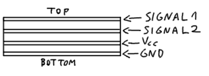
* for high quality hobbiest boards with very low noise/EMI: 4 layers with seperate ground/Vcc planes.
something along the lines of this i assume:
* for cheaper quality boards: 2 layers with a Grid of Ground traces.
something like this? :
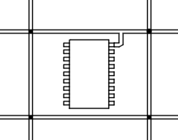
note that the vertical and horizonal lines are not on the same side, but connected via vias.
what confuses me about this is what is the size of the grid supposed to be? i assume a square shape is always the best and it should be atleast the width of the largest IC + a bit extra space.
like this maybe? :
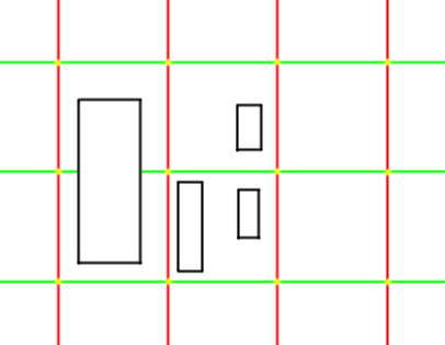
and what about Vcc?
couldn't you make a grid like this to have GND and Vcc always next to eachother? or would that somehow make noise/EMI worse? because this is almost a breadboard at this point.
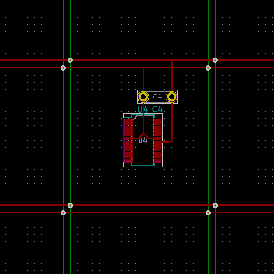
* alternative cheap option with 2 layers (i saw it online a lot)
Have 1 layer be a ground plane, and do everything else on the other layer, if vias have to be used the trace on the GND side should be as short as possible.
* standard Hobbiest starter option:
Just let Free/AutoRouting do it, make sure there are no ground loops or similar.
it works for small projects
this is basically what i got from this.
as people said before i can go for the more advanced things to make sure it works, but it likely will also work without them unless i really test my luck with large/fast/complex boards
I could go for the grid one, (only GND or with Vcc in the grid like i showed?), but it would require me to completely redo the layout as i need to manually place the grid and make sure it fits all components. then FreeRouting could do all the signal lines.
Re: Starting with my first SBC Project, Plans and Confusions
Usually with a 4-layer board, the ground and power planes are put on the inner, hidden layers, with signals on the outer layers. If nothing else this helps to reduce crosstalk between signals.
Your grid layout looks reasonable, though I would use thicker traces (say 50mil) for power and ground than for signals. There's nothing to prevent you leading a power trace up the middle of a DIP IC, or spacing the traces unevenly; the important factor is the distance between any given signal trace and its return paths (Vcc when pulling up, GND when pulling down).
You'll quickly find, even with a 4-layer board, that using one side of the board for vertical traces and the other for horizontal ones makes layout much easier. Installing a power grid effectively enforces that. Power and ground planes give you more freedom to deviate when appropriate.
Re: Starting with my first SBC Project, Plans and Confusions
Chromatix wrote:
Usually with a 4-layer board, the ground and power planes are put on the inner, hidden layers, with signals on the outer layers. If nothing else this helps to reduce crosstalk between signals.
Your grid layout looks reasonable, though I would use thicker traces (say 50mil) for power and ground than for signals. There's nothing to prevent you leading a power trace up the middle of a DIP IC, or spacing the traces unevenly; the important factor is the distance between any given signal trace and its return paths (Vcc when pulling up, GND when pulling down).
You'll quickly find, even with a 4-layer board, that using one side of the board for vertical traces and the other for horizontal ones makes layout much easier. Installing a power grid effectively enforces that. Power and ground planes give you more freedom to deviate when appropriate.
Your grid layout looks reasonable, though I would use thicker traces (say 50mil) for power and ground than for signals. There's nothing to prevent you leading a power trace up the middle of a DIP IC, or spacing the traces unevenly; the important factor is the distance between any given signal trace and its return paths (Vcc when pulling up, GND when pulling down).
You'll quickly find, even with a 4-layer board, that using one side of the board for vertical traces and the other for horizontal ones makes layout much easier. Installing a power grid effectively enforces that. Power and ground planes give you more freedom to deviate when appropriate.
also what about the idea of having both GND and Vcc in the Grid? like i showed in the picture? is it a good idea or somehow bad?
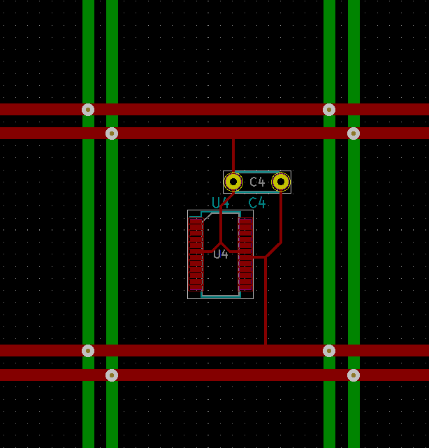
fixed version