My6502 - A 74-Series 6502

For discussing the 65xx hardware itself or electronics projects.
vfxsoup
Posts: 34
Joined: 30 Sep 2019

Re: My6502 - A 74-Series 6502

Post by vfxsoup »

Hi all. Happy new year!

I've been giving some thought to the physical construction of my computer. I'm thinking that there'll be a longish bus board that has the five buses (WB, RB, ADL, ADH, and DB) running in parallel, along with tracks for power and clocks. If power is +5v, GND, and clocks are CLK, PHI1, PHI2, then the board will essentially be 45 tracks, and for prototyping I could use some stripboard (like this https://www.ebay.co.uk/itm/Stripboard-1 ... 3074484745). Each card sits vertically, having right-angled Dupont headers for attaching to the bus board.

I've also been designing the register card, abandoning the dual-register-per-card idea in favour of a much simpler single 8-bit register. I also decided to simplify things somewhat and go with using a pair of 74HC161 chips for each register, since they will work nicely as both static registers and counters. The idea here is that I can use one card for each register, with the exception of the status register, hence the generic design.

Here's the schematic:
Image

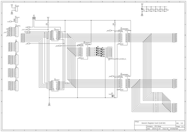
The '161s take their input from the W bus directly, and output to the display LEDs via a 74HC541 buffer. The reason for this is so I can turn the LEDs on and off globally using the _DISP control wire if running in fast mode, as well as ensuring the signal integrity due to power draw from the LEDs.

Each register can but output to two of the three output buses. The outputs are buffered using a pair of 74HC245s (or 541s if preferred as they have almost identical pinouts except for pin 1. A pullup resistor sets pin 1 on the '245 to direction A->B, and using the jumper pulls the pin to ground to turn on one of the OE controls if using the '541). I happen to have quite a few '245 chips, which is why I'm using them but it was easy enough to add in the flexibility to use the unidirectional buffer if needed.

A series of jumpers sets the ADH output to use either one of the two output buffers.

I'll be prototyping it using breadboards soon to make sure it works.

As for the Stack Register, I've been considering using the 74LS169 as suggested by Deiter. Conceptually it can replace the '161s directly with no modifications to the circuitry, because the pinout is identical. The _CLR/_DEC control wire will either be floating for the majority of cards (the _CLR control is reserved for another time...), so pin 1 (_MR) on the '161 is pulled high by R3, or set appropriately for the Stack Register. Aside from the LS169's eye-wateringly high power consumption (100mW!) and cost (£1.50 per chip!) the obvious concern is mixing TTL with CMOS. Am I correct in thinking that replacing the LED and output buffers with HCT versions will allow this to work? I'm using only 5V for power, input voltage will be high enough to drive the TTL. The HCT chips can take TTL level inputs and output VCC, so the buses will be driven at the same voltages as from the all-CMOS cards. Is that right?

[EDIT]I've just noticed that the LS169 uses active low count enable pins, whereas the HC161's are active high - same for the RCO. So the circuit will require a small rework but nothing too complex[/EDIT]

As usual all comments and suggestions gratefully received.

Thanks, Christian
Last edited by vfxsoup on Sun Jan 12, 2020 7:44 pm, edited 1 time in total.
User avatar
BigDumbDinosaur
Posts: 9428
Joined: 28 May 2009
Location: Midwestern USA (JB Pritzker’s dystopia)
Contact:

Re: My6502 - A 74-Series 6502

Post by BigDumbDinosaur »

Anyway to post that in monochrome?
x86?  We ain't got no x86.  We don't NEED no stinking x86!
vfxsoup
Posts: 34
Joined: 30 Sep 2019

Re: My6502 - A 74-Series 6502

Post by vfxsoup »

BigDumbDinosaur wrote:
Anyway to post that in monochrome?
Done. I updated the original post with the mono version.
User avatar
Dr Jefyll
Posts: 3526
Joined: 11 Dec 2009
Location: Ontario, Canada
Contact:

Re: My6502 - A 74-Series 6502

Post by Dr Jefyll »

vfxsoup wrote:
Done. I updated the original post with the mono version.
For future reference, on this forum you don't need to use a third-party host for images. You'll find it more convenient to post as an attachment, and also the result is more permanent. :wink:
Quote:
using a pair of 74HC161 chips for each register
For this sort of project, often the '163 counter is preferable to the '161. The 163 offers synchronous load and clear, and of course counting is also synchronous. When all changes occur synchronously it's usually a cleaner way of doing things. Just a suggestion. :)

ETA: synchronous is cleaner and can run faster because circuit timing simply involves...
  1. setting inputs up for the next clock edge, and
  2. allowing changes resulting from the clock edge to propagate... which is what results in (a).
Asynchronous inputs complicate matters because they act immediately, and thus have no tolerance for glitches. It becomes necessary to gate the asynchronous inputs so they're inactive while changes propagate.

-- Jeff
In 1988 my 65C02 got six new registers and 44 new full-speed instructions!
https://laughtonelectronics.com/Arcana/ ... mmary.html
vfxsoup
Posts: 34
Joined: 30 Sep 2019

Re: My6502 - A 74-Series 6502

Post by vfxsoup »

Dr Jefyll wrote:
For future reference, on this forum you don't need to use a third-party host for images.
Noted, thanks.
Quote:
For this sort of project, often the '163 counter is preferable to the '161
Ah OK, interesting. I have a stack of '161s so I'll have to go with them for now (also Farnell, from whom I buy all my chips, no longer sell the '163). I'm not planning on using the clear input anyway really so I'm hoping it won't be a problem. I've just added the CLR input for futureproofing, and I can always swap out the '161s for '163s later as they have an identical pinout.

I'm struggling to finalise my up/down counter solution though. The 74HC191 (I discovered today) has no synchronous load, and I don't want to start building extra circuitry to do edge detecting, so the 74LS169 seems to be the best option. What do you think about mixing TTL and CMOS using the HCT varieties as I mentioned above? I saw you can also pull up each TTL output with a 2k2 resistor, which presumably raises the voltage to CMOS input levels, and this would negate the need to use HCT flavours.

Thanks, Christian
User avatar
Dr Jefyll
Posts: 3526
Joined: 11 Dec 2009
Location: Ontario, Canada
Contact:

Re: My6502 - A 74-Series 6502

Post by Dr Jefyll »

vfxsoup wrote:
I'm not planning on using the clear input anyway really so I'm hoping it won't be a problem.
OK, good -- you're alright, then. But for reference here (below) is an illustration of how a circuit could be adapted if that were necessary. It's a solution to be used with caution, however, as it limits the maximum clock rate and indeed may fail based on assumptions about the relative speeds of the gate and the counter.

The gate is provided to ensure /CLR is active (ie, low) only during the latter half of every clock cycle. The first half of every clock cycle isn't safe, because this chip and others will be in a state of flux in the instant following the rise of CLK. This could briefly produce an erroneous Clear command.
counter example.png
counter example.png (5.27 KiB) Viewed 1944 times
Quote:
The 74HC191 (I discovered today) has no synchronous load, and [...] the 74LS169 seems to be the best option. What do you think about mixing TTL and CMOS using the HCT varieties as I mentioned above?
Well, you could use 'HC191 if you were willing to gate the load input just as /clear is gated above. But I recommend you go with the 'LS169 and use pullups as you suggest.

-- Jeff

ps- for posterity, I'm posting your diagram :)
Attachments
Schematic-My6502-Register-Board-Register-Card-Schematic-20200112163411-mono.jpg
In 1988 my 65C02 got six new registers and 44 new full-speed instructions!
https://laughtonelectronics.com/Arcana/ ... mmary.html
vfxsoup
Posts: 34
Joined: 30 Sep 2019

Re: My6502 - A 74-Series 6502

Post by vfxsoup »

Dr Jefyll wrote:
...for reference here (below) is an illustration of how a circuit could be adapted if that were necessary.
I'm curious about the gate that's in your illustration - doesn't inverting the inputs of a NAND gate technically turn it into an OR gate? What is the purpose of the inverted inputs, and how would you achieve this without using couple of inverters like a 74xx04? As a relative newbie I'm just interested why the gate is illustrated in this way.

Thanks.
User avatar
Dr Jefyll
Posts: 3526
Joined: 11 Dec 2009
Location: Ontario, Canada
Contact:

Re: My6502 - A 74-Series 6502

Post by Dr Jefyll »

vfxsoup wrote:
doesn't inverting the inputs of a NAND gate technically turn it into an OR gate?
Yes, that's right. A NAND (ie, an AND with its output inverted) can be considered an OR if its inputs are also inverted.

I had a choice between drawing the circuit in two different ways.
logic snippet.png
logic snippet.png (2.23 KiB) Viewed 1831 times
I think you know the rule. An AND can be drawn as an OR with all its inputs & outputs inverted. Likewise an OR can be drawn as an AND with all its inputs & outputs inverted. My diagram below shows 2-input gates but the same applies for 3-input gates, 4-input and so on. See De Morgan's Law.
logic equivalents.png
logic equivalents.png (1.22 KiB) Viewed 1831 times
I chose to illustrate using the AND symbol (with inverted I/O) because I believe AND more clearly communicates the intent. Ie, the gate's output is inactive unless /CLR-ENABLE is low "AND" CLK is low. But this is a matter of preference. Some would rather see an illustration of an OR gate (without inverted I/O).

BTW, on the subject of synchronous loading and clearing of a counter/register, the usual arrangement is like that found in the 74xx377. This is an octal register similar to '374, except a rising edge on the clock input will produce no effect unless the /E input is low.
'377 internal logic.png
What's notable is how there's no fussing with the clock signal itself. Instead, each of the flip-flops is fed by a multiplexer, and, at times when the /E input is high, the multiplexer simply feeds the FF's existing state back to its D input -- that's why no change occurs even though the FF does in fact get clocked. :!:

It's a tidier way of doing things. With this arrangement, the state of the /E input is unimportant right up until almost immediately before the clock edge. IOW, it's well able to tolerate glitches (unlike asynchronous inputs). For new data, let the mux input new data. For no-change, feed the FF's state back to itself. To clear, the mux feeds the FF with logic low.

Counters offer additional inputs to the mux; likewise, shift registers. :)

-- Jeff
Last edited by Dr Jefyll on Tue Jan 21, 2020 12:16 am, edited 3 times in total.
In 1988 my 65C02 got six new registers and 44 new full-speed instructions!
https://laughtonelectronics.com/Arcana/ ... mmary.html
vfxsoup
Posts: 34
Joined: 30 Sep 2019

Re: My6502 - A 74-Series 6502

Post by vfxsoup »

Thanks for the explanation Jeff.

I'm to-ing and fro-ing with my register circuit designs. In fact I've reverted to using the 74HC377 (as used in your explanation above) for the static version of the card, since I have a lot of these chips in stock with little else to do with them! I'm trying to decide whether to have two cards, one for static, one for counter, or use the static card with a small, panelized daughterboard that takes the HC161/LS169. The track layout doesn't seem to facilitate a ground fill because of the many tracks crossing, so it may have to be a four layer board, which increases the price somewhat. I'll post some updated schematics and PCB layouts soon.
vfxsoup
Posts: 34
Joined: 30 Sep 2019

Re: My6502 - A 74-Series 6502

Post by vfxsoup »

A brief update.

I've modified all the "MicroCodeAssembler" and the "ControlUnit" code in the emulator to move the fetch-next-instruction to be the last thing in each instruction, as advised. I realised this would be advantageous for a couple of reasons, but one unexpected bonus was that I've clawed back a microcode instruction (recall that my ROMs were choc full!). Now that the MI_INST_END micro-instruction has become obsolete I've been able to replace it with the ALU shift right micro-instruction, which in turn removes the ALU input hack and may save me a couple of chips. The update isn't fully tested, but the Fibonacci sequence program still works OK. The update has been committed to GitHub.

I've also been looking at the circuit design for the Status Register. It was a bit of a challenge because of the need to only update the relevant bits rather than the whole byte. I've still got no idea how the B-bit gets set but we can look at that later.

Finally I've been wondering how to implement the reset/hardware interrupt sequences. Where would one store these sequences and how do they get executed? I guess I'm struggling with the concept of what the Program Counter & address pointers do during these moments. Is there a separate ROM for them, and do they just execute the standard instructions (I can assume that the hardware interrupts are just variations of BRK)? Currently my emulator does a horrible hard-code of the reset to fetch the first instruction.
User avatar
ttlworks
Posts: 1464
Joined: 09 Nov 2012
Contact:

Re: My6502 - A 74-Series 6502

Post by ttlworks »

IIRC the C74-6502 TTL CPU runs the BRK microcode when it comes to RES, NMI, IRQ by forcing the instruction register to $00,
and the vector address for the address bus is generated by hardware.
vfxsoup
Posts: 34
Joined: 30 Sep 2019

Re: My6502 - A 74-Series 6502

Post by vfxsoup »

ttlworks wrote:
IIRC the C74-6502 TTL CPU runs the BRK microcode when it comes to RES, NMI, IRQ by forcing the instruction register to $00,
and the vector address for the address bus is generated by hardware.
Of course. It's obvious now!

I misunderstood when...
GARTHWILSON wrote:
...one of the first things your reset routine should do is LDX #$FF, TXS.
...thinking that this mysterious reset routine was something that happened internally to the CPU (silly now I think about it!). The reset routine is obviously somewhere in ROM, and separate from the CPU itself. Doh!

Because my microcode can have up to 4 variants I can adjust the BRK instruction if necessary for each of RES/NMI/IRQ. AFAIK it's just this pesky 'B' bit and whether or not the I flag gets set. As with the C-74 the actual vector addresses will be set by hardware.

So during an actual BRK instruction (i.e. a software interrupt), how does the B bit get set? Hansen's block diagram doesn't have a control wire for setting the bit (and neither does my emulator).

In fact, how does the CPU set the initial state of the Status Register (bits 4 and 5 on, and the rest off)? Is that also something that happens during the reset routine?

Thanks!
User avatar
Drass
Posts: 428
Joined: 18 Oct 2015
Location: Toronto, ON

Re: My6502 - A 74-Series 6502

Post by Drass »

vfxsoup wrote:
Because my microcode can have up to 4 variants I can adjust the BRK instruction if necessary for each of RES/NMI/IRQ.
Have a look at C74-6502 Card A Schematic at CGL (top right, coordinate A.7). CGL stands for Constant Generator Low. It’s a 74AC541 used to put the low-byte of the vectors address on the address bus during the BRK sequence.
Quote:
So during an actual BRK instruction (i.e. a software interrupt), how does the B bit get set?
The C74-6502 has an “interrupt in progress” flip-flop (see C74-6502 Card B Schematic F.12 “Interrupt Detect INT.INP”). It is set during a SYNC cycle if any interrupt is pending, and cleared at the end of the BRK microcode sequence. All “PUSH P” operations uses /INT.INP as the value for the B-Flag. (See Card B Schematic H.9 “P Register PBUF” 74AC541 pin 6).
Quote:
In fact, how does the CPU set the initial state of the Status Register (bits 4 and 5 on, and the rest off)? Is that also something that happens during the reset routine?
The P register is not explicitly initialized. Bit 4 is the B Flag as above and Bit 5 is always on. The BRK sequence will set the I-Flag (and clear the D-flag on the 65C02 IIRC). Other status bits are only set as instructions execute.

The C74-6502 is allowed to run free when the /RES pin is held low on power-up, with writes to memory disabled (R/W is forced high). Hence, the status register will simply reflect the results of the most recent instructions which were executed prior /RES going high and the initial BRK microcode sequence being invoked.
C74-6502 Website: https://c74project.com
vfxsoup
Posts: 34
Joined: 30 Sep 2019

Re: My6502 - A 74-Series 6502

Post by vfxsoup »

Hello everyone. It's been a while. Firstly a very belated thanks Drass for your response - it was very helpful in allowing me to better understand the "B" bit and how it works.

So, bigish news - I've been working hard on the My6502 emulator since I felt I'd neglected it somewhat recently. I've now written the microcode for every MOS6502 instruction! I've also made sure that all memory access happens during PHI2, as per the real thing, which I'm sure will come into play when I start working on the display hardware. The "Snake" game over at Easy6502 has been a great help in debugging various aspects, including branching and carry flag use, and now my emulator runs the game perfectly, which I'm very proud of! I also ran BigEd's ADC/SBC test program from this thread and it passed!

The emulator now has a "turbo" mode, which basically just runs the component/clock updates thousands of times per frame. However the fastest I can manage on my home PC is about 24KHz! I should probably attempt to run one of the big tests like Klaus Dormann's test but given that it takes 52 seconds at 2MHz, I'll be running it for about 72 agonising minutes at my paltry speeds. I need to get my head around it first though, including assembling it and figuring out how it reports success or failure.

Other things of note, the reset (and presumably other hardware interrupts) seem to be working properly now, and I've started to annotate/tidy up the code a bit. Expect a new commit soon.

Christian
Attachments
Latest version
Latest version
Easy6502 Snake game running on My6502
User avatar
BigEd
Posts: 11464
Joined: 11 Dec 2008
Location: England
Contact:

Re: My6502 - A 74-Series 6502

Post by BigEd »

Nice update, thanks!
Post Reply