In another
thread, BigEd made a remark concerning clock skew.
Probably pictures would help here a lot more than words!
As the topic has arisen more than once I decided to have a go at this.
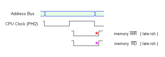
- timing skew (mem late).png (2.83 KiB) Viewed 2430 times
Here (above) is what you'll see in a typical 6502 or 65C02 setup where the memory /WR and /RD signals are qualified by the CPU clock. I've shown the address bus changing instantly when Phi2 goes low although in fact there is some delay. We can discuss that detail (and others such as the delay between Phi2 IN and Phi2 OUT) later, but right now an overview seems in order, and my goal is to show what must ultimately go wrong when /RD and /WR are delayed "too much." Too much delay means you can end up reading from or writing to an incorrect address at the end of the cycle. A few ns of this
might be tolerable, but...

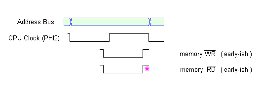
- timing skew (mem early).png (2.58 KiB) Viewed 2430 times
The hazards seem less pronounced when /RD and /WR are early. Toward the end of a read cycle, memory will tristate the data bus before the CPU has closed its input latch which accepts the data, but that's harmless (assuming the DC loading on the data bus is negligible and capacitance can be relied upon to sustain the logic levels, as no other device is driving the bus after Phi2 falls). (nb: comment not applicable to 65816!) The other hazards are simply reduced time allowances as seen from memory's POV. But IC specifications tend to be conservative, and to create a problem I think you'd have to make /RD and /WR very early indeed. However, taken too far...
- reads will commence before the address is valid, which is harmless provided there's enough time after it becomes valid.
- writes will commence before the data is valid, which is harmless provided there's enough time after it becomes valid.
- writes will commence before the address is valid. A few ns of this
might be tolerable, but...
Comments/additions/corrections welcome,

Jeff


