
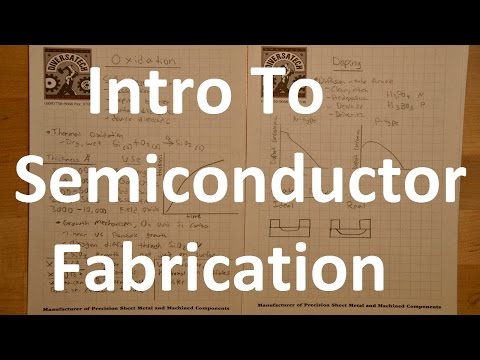
Semiconductor Fabrication Basics - Thin Film Processes, Doping, Photolithography, etc.
More on his web site (http://sam.zeloof.xyz/):
- Homemade Insulated Gate Field Effect Transistor (MOSFET)
- Introduction to Semiconductor Fabrication at Home
- High Vacuum Experiments – Physical Vapor Deposition, Plasma Cleaning/Etching, etc.
- Homemade Photovoltaics – DIY Silicon PN Junction Solar Cells
- Maskless Photolithography with DLP Projector – 10um Feature Sizes
[1] We've had one or two excursions as to whether custom chips could be designed and made or whether a small fab could be constructed. My own take is that fabrication is very capital-intensive. With older equipment which should be cheaper you can make only the older less dense technologies. Without high volume, your chips will need to be priced in the thousands, and you are going to struggle to find customers with such deep pockets. Design is also rather expensive: to get from a sketch to mask data takes a lot of effort, skill, and tools. To get from mask data to masks is expensive too.
