6502.org Forum  Projects  Code  Documents  Tools  Forum
It is currently Sun Nov 24, 2024 2:22 am

All times are UTC


Post new topic Reply to topic  [ 19 posts ]  Go to page 1, 2  Next
Author Message
 Post subject: Why, oh lord why?
PostPosted: Thu Jan 18, 2018 1:49 pm 
Offline
User avatar

Joined: Fri Dec 12, 2008 10:40 pm
Posts: 1007
Location: Canada
Hey guys,

So, I built the following circuit up on a solderless breadboard. I have included a schematic of the logic implemented in the GAL and a picture of my BB layout.

Here's the thing. My intention was to use this with a R65C02, so all the other chips are CMOS. The 2 74 series chips are AC (74ACXXX), the RAM, EPROM, ACIA and GAL are all CMOS. The clock speed is 1.8432MHz and the propagation delay to RAM or EPROM select it measured at 12ns and 20ns to the ACIA or memory register (74AC374) select. The EPROM and RAM are fairly fast devices @ 120ns. The GAL implements a PHI2 gated R/~W with a 12ns delay for the RAM. The EPROM contains a mini-monitor and EhBASIC 2.22. The ACIA is connected to a PC through a TTL to RS23 module that incoprporates a MAX232 (seen in the photo). I've checked the input and output logic levels of every chip in the circuit from their datasheets - they should be absolutely compatible. Everything should be honky dory, right?

Except it's not.

Using a R65C02-4 it has issues. Sometimes I can get a short program loaded in, but running it will produce errors and corrupt memory. Using a WD65C02 (modified to be plugable into a 6502 socket) it does not work at all - well I get a single space character output at the ACIA on reset - pffft!

However, using a good old NMOS 6502A it works like a charm.

What lunkhead thing am I doing wrong that prevents the CMOS CPUs from working?

Any help would be appreciated.


Attachments:
File comment: Breadboard
OMS-01A.jpg
OMS-01A.jpg [ 253.72 KiB | Viewed 5869 times ]
File comment: GAL Logic
OMS-01MM.jpg
OMS-01MM.jpg [ 175.81 KiB | Viewed 5869 times ]
File comment: Schematic
OMS-01.jpg
OMS-01.jpg [ 494.35 KiB | Viewed 5869 times ]

_________________
Bill
Top
 Profile  
Reply with quote  
 Post subject: Re: Why, oh lord why?
PostPosted: Thu Jan 18, 2018 3:23 pm 
Offline

Joined: Sat Nov 26, 2016 2:49 pm
Posts: 27
Location: Tejas
I'd suggest yours are noise problems. Good decoupling at the devices themselves is mandatory and you may need more extensive multi-stage decoupling at/near the devices. Protoboards are notorious for noise all by themselves and when you add in CMOS edge rates you've probably got quite a stew going on there.


Top
 Profile  
Reply with quote  
 Post subject: Re: Why, oh lord why?
PostPosted: Thu Jan 18, 2018 10:56 pm 
Offline
User avatar

Joined: Fri Dec 12, 2008 10:40 pm
Posts: 1007
Location: Canada
I do have 2 .1uf monolithic ceramic caps at each device as well as 10uf electrolytics at the top of each rail.

It is noisy though, but no more than I've seen other systems - like the Apple IIe enhanced which uses the R65C02 without issue and will run just fine on my modified W65C02.

I could put 1uf and .1uf monolithic ceramics beside each .1 to see if that helps, but I have my doubts. I'll try it tomorrow.

_________________
Bill


Top
 Profile  
Reply with quote  
 Post subject: Re: Why, oh lord why?
PostPosted: Thu Jan 18, 2018 11:16 pm 
Offline
User avatar

Joined: Fri Aug 30, 2002 1:09 am
Posts: 8546
Location: Southern California
Solderless breadboards are the worst of all worlds for performance for this kind of thing, and bypassing is only a small part of the problem; nevertheless, good bypassing involves connecting the capacitors from an IC's Vcc pin to its ground pin with the connections as short as possible, not out at the rails like what I see in the picture. If you can put the capacitors over the ICs rather than making the connections go out and way around, it will help. Also, make the ground and Vcc connections from one IC to another (including the oscillator) as short and direct as possible. That all may not be enough though. The faster part has faster rise and fall times than the old NMOS one does, which will cause more ringing and groundbounce in such non-ideal layouts.

_________________
http://WilsonMinesCo.com/ lots of 6502 resources
The "second front page" is http://wilsonminesco.com/links.html .
What's an additional VIA among friends, anyhow?


Top
 Profile  
Reply with quote  
 Post subject: Re: Why, oh lord why?
PostPosted: Fri Jan 19, 2018 3:25 pm 
Offline
User avatar

Joined: Fri Dec 12, 2008 10:40 pm
Posts: 1007
Location: Canada
Some of those chips are pretty big and running the cap over the chip diagonally may actually lengthen the distance from the power pins. Not to mention I don't have any caps with leads long enough to span a 32 pin chip diagonally. However, I could snug things up a bit at the risk of lengthening one path by a bit. I think I have some axial lead caps that might span up to 18 or 20 pin packages.

This breadboard, despite being a US made 'quality' unit does have rather long distances to span from the chip leads to the power rails. I have some Chinese made units that have much shorter distances from rails to chips, but moving the project would be a last resort at this point. I'll know better next time.

They should design these things with the power rails between the dip leads (where the chanels are) and utilize a PCB base panel with power planes to distribute power to the solderless panels.

Another issue I'm dealing with is, even with power completely removed from the project I'm picking up 500mv peak to peak noise (the majority of what I'm measuring) between the power rails. I am under the belief this is coming from the LED lighting installed throughout the room I'm using. Has anyone else seen this? I'll earth the aluminum base to try to help with this.

IN any case, thanks for the responses. I'll do my best to improve the bypassing, but as it is now, most of what I want to accomplish with this phase can be done with the NMOS processor.

One more question. It seems like solderless breadboards are not the hot setup for experimenting with anything above 1 or 2 MHz. What do the rest of you use when doing experiments at higher clock speeds and with faster devices?

Edit: Changed 'substrate' to 'bass panel'

_________________
Bill


Last edited by BillO on Fri Jan 19, 2018 4:28 pm, edited 2 times in total.

Top
 Profile  
Reply with quote  
 Post subject: Re: Why, oh lord why?
PostPosted: Fri Jan 19, 2018 3:56 pm 
Offline
User avatar

Joined: Wed Aug 17, 2005 12:07 am
Posts: 1250
Location: Soddy-Daisy, TN USA
BillO wrote:
One more question. It seems like solderless breadboards are not the hot setup for experimenting with anything above 1 or 2 MHz. What do the rest of you use when doing experiments at higher clock speeds and with faster devices?


I'm guessing most of the guys around here that want to build faster circuits use wire wrap and/or custom PCB's.

Despite some design flaws on my latest PCB, they are ridiculously cheap these days. Especially for anything under 100x100mm.

_________________
Cat; the other white meat.


Top
 Profile  
Reply with quote  
 Post subject: Re: Why, oh lord why?
PostPosted: Fri Jan 19, 2018 9:36 pm 
Offline
User avatar

Joined: Fri Aug 30, 2002 1:09 am
Posts: 8546
Location: Southern California
BillO wrote:
Some of those chips are pretty big and running the cap over the chip diagonally may actually lengthen the distance from the power pins.

Leads have inductance, and you need to minimize the lead length in the bypass capacitors between the power pin and the ground pin, splicing on extra wire if necessary to make the span. Oh how I wish they had foreseen the future rising edge rates and clock speeds when they came up with pinouts, and put the power and ground pins in the middle of the IC not out at the corners! I have worked with more-modern ones that put a power and ground pin right together on each side of the IC, as close as possible to the die, ie, the actual silicon chip inside, to minimize inductance where it's most important to minimize.

You can still have bypass capacitors at the power rails too of course.

Quote:
They should design these things with the power rails between the dip leads (where the chanels are) and utilize a PCB base panel with power planes to distribute power to the solderless panels.

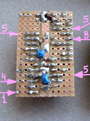
What I've often done with solder-type breadboards (which I use when there's a lot of analog circuitry involved) is to put adhesive copper foil down the middle for ground. Here's the idea, although this one is purely analog (no digital), for work:
Attachment:
BBsigsSolderSide.jpg
BBsigsSolderSide.jpg [ 94.69 KiB | Viewed 5745 times ]

Most of the components are on the other side; but it became convenient and helpful to put some on the solder side. It works out particularly well for bypass capacitors, since the ground pin can go to the copper ground strip directly with a super-short connection, and the Vcc pin can just have a leadless chip capacitor soldered between its solder pad and the ground copper ground strip. There aren't any chip capacitors on this particular board, but it's not uncommon for me to put them on other boards.

Quote:
Another issue I'm dealing with is, even with power completely removed from the project I'm picking up 500mv peak to peak noise (the majority of what I'm measuring) between the power rails. I am under the belief this is coming from the LED lighting installed throughout the room I'm using. Has anyone else seen this? I'll earth the aluminum base to try to help with this.

50/60Hz mains frequency, or MHz stuff?

Quote:
One more question. It seems like solderless breadboards are not the hot setup for experimenting with anything above 1 or 2 MHz. What do the rest of you use when doing experiments at higher clock speeds and with faster devices?

Like cbmeeks said, wire-wrap or custom PCBs. The 6502 primer has a page answering wire-wrap questions and doubts, at http://wilsonminesco.com/6502primer/WireWrap.html .

_________________
http://WilsonMinesCo.com/ lots of 6502 resources
The "second front page" is http://wilsonminesco.com/links.html .
What's an additional VIA among friends, anyhow?


Top
 Profile  
Reply with quote  
 Post subject: Re: Why, oh lord why?
PostPosted: Fri Jan 19, 2018 9:44 pm 
Offline

Joined: Sat Jun 04, 2016 10:22 pm
Posts: 483
Location: Australia
CBMeeks is certainly right about the price. DirtyPCBs will make a 4-layer 100x100mm board for about US$45(shipping is about US$12 on top of that, at least to AU). It's cheaper if you only need 2-layer and/or smaller than 50mm in both directions. I can't yet speak for the quality of the boards, as mine only shipped yesterday afternoon.

Everyone else I've looked at starts at $100+. But I haven't looked at too many.


Top
 Profile  
Reply with quote  
 Post subject: Re: Why, oh lord why?
PostPosted: Fri Jan 19, 2018 10:22 pm 
Offline
User avatar

Joined: Fri Aug 30, 2002 1:09 am
Posts: 8546
Location: Southern California
The 6502 primer also has a page on custom PC boards, at http://wilsonminesco.com/6502primer/CustomPCB.html, with a lot of good links, including to relevant topics on this forum, and to pages about CAD (including free CAD packages).

_________________
http://WilsonMinesCo.com/ lots of 6502 resources
The "second front page" is http://wilsonminesco.com/links.html .
What's an additional VIA among friends, anyhow?


Top
 Profile  
Reply with quote  
 Post subject: Re: Why, oh lord why?
PostPosted: Sat Jan 20, 2018 6:59 pm 
Offline
User avatar

Joined: Fri Dec 12, 2008 10:40 pm
Posts: 1007
Location: Canada
Thanks for all the suggestions folks! Much appreciated.

I did find some axial lead bypass capacitors at a (fairly) local parts shop with extraordinarily long leads. I'll be able to run them over the 32 and 28 pin packages with ease!

GARTHWILSON wrote:

50/60Hz mains frequency, or MHz stuff?

Fairly broad spectrum with a peak around 23KHz.

_________________
Bill


Top
 Profile  
Reply with quote  
 Post subject: Re: Why, oh lord why?
PostPosted: Wed Jan 24, 2018 7:07 pm 
Offline
User avatar

Joined: Fri Dec 12, 2008 10:40 pm
Posts: 1007
Location: Canada
So I tired all the suggestions I could up to and including soldering the cap right to the IC pins (where there was not enough holes in the breadboard or the chip needed to be removed often - eprom) and I have had some measure of success. The measured noise between Vcc and gnd is down 6db. The R65C02 does no better than before but the W65C02 works now - well at least as good as the R65C02. I am also able to push the NMOS 6502A to 3.8MHz where the limit was 2.5 before. I think it maybe the 65C51 crapping out. I need to try the W65C51 (with teh appropriate delay in the transmit routine) but I'll wait until I transfer the circuit to a stable base. I have had good luck with the boards pictured.

Attachment:
OMS-PBD-A.jpg
OMS-PBD-A.jpg [ 191.23 KiB | Viewed 5637 times ]


Attachment:
front.jpg
front.jpg [ 164.13 KiB | Viewed 5637 times ]

_________________
Bill


Top
 Profile  
Reply with quote  
 Post subject: Re: Why, oh lord why?
PostPosted: Fri Jan 26, 2018 5:59 pm 
Offline

Joined: Sat Dec 13, 2003 3:37 pm
Posts: 1004
How is a board like that used?

On a bread board, you have some bus lines on the edge (where all of the holes are tied together) with a bunch of holes in a grid, where lines of 5 are all connected together.

So, if you wanted to connect two components, you just need to ensure that they share a 5 hole line, or that there's a jumper from one line to the other. Finally, there are solder versions of the breadboards where you solder the components to the board, rather than just shove them in.

In these boards, you have couple of "bus" lines, but all of the other holes are not connected at all. So, how do you connect components?


Top
 Profile  
Reply with quote  
 Post subject: Re: Why, oh lord why?
PostPosted: Sat Jan 27, 2018 12:46 pm 
Offline

Joined: Wed Jan 08, 2014 3:31 pm
Posts: 578
Those prototyping boards look really useful. Where did you get them?


Top
 Profile  
Reply with quote  
 Post subject: Re: Why, oh lord why?
PostPosted: Sat Jan 27, 2018 6:18 pm 
Offline

Joined: Sat Jan 02, 2016 10:22 am
Posts: 197
whartung wrote:
. So, how do you connect components?


Either wire wrap or in my case point to point soldering on the back with 30 awg wire.


Top
 Profile  
Reply with quote  
 Post subject: Re: Why, oh lord why?
PostPosted: Wed Jan 31, 2018 8:45 pm 
Offline
User avatar

Joined: Fri Dec 12, 2008 10:40 pm
Posts: 1007
Location: Canada
whartung wrote:
How is a board like that used?

On a bread board, you have some bus lines on the edge (where all of the holes are tied together) with a bunch of holes in a grid, where lines of 5 are all connected together.

So, if you wanted to connect two components, you just need to ensure that they share a 5 hole line, or that there's a jumper from one line to the other. Finally, there are solder versions of the breadboards where you solder the components to the board, rather than just shove them in.

In these boards, you have couple of "bus" lines, but all of the other holes are not connected at all. So, how do you connect components?


There are two separate power buses each with two lines, one on the left hand half of the board and one on the right. Component pads are arranged like 4 solderless breadboards. They are connected on the bottom of the board with .08" traces with a solder mask. Holes are plated through to allow for mounting components on either side. There are connector points for .2" screw terminals and for both double row and single row .1 spacing headers. There are 2 power supplies preconfigured to use LM78XX regulators with LED pilot lights. As well there are pads for 6 LED indicators with resistors, 2 pushbutton switches, a 3.5mm stereo jack, two barrel type power jacks, a 9-pin D connector and two areas for configuring 3-wire sensor/actuator headers.

Maybe the pictures here will give you a better idea.
Attachment:
Populated 3.jpg
Populated 3.jpg [ 145.08 KiB | Viewed 5511 times ]

Attachment:
Populated 1.jpg
Populated 1.jpg [ 193 KiB | Viewed 5511 times ]

_________________
Bill


Top
 Profile  
Reply with quote  
Display posts from previous:  Sort by  
Post new topic Reply to topic  [ 19 posts ]  Go to page 1, 2  Next

All times are UTC


Who is online

Users browsing this forum: Google [Bot] and 65 guests


You cannot post new topics in this forum
You cannot reply to topics in this forum
You cannot edit your posts in this forum
You cannot delete your posts in this forum
You cannot post attachments in this forum

Search for:
Jump to: