All I really want from the uVGA is a bridge to the monitor. Any other features are just gravy. I actually plan to roll my own font.
I'm curious as to which uVGA version you used? I have the III, and the documentation seems to imply it does a lot. Much more than I plan to use.
I had the µVGA II, which is essentially the same device. It does do a lot, but cannot generate a cursor in hardware, which was a deal-breaker for me. We had some discussion around here several years ago about how one might simulate a cursor in software but never did come up with a viable method. As I noted, text displays are not really the µVGA's forte—writing a single character to the screen involves issuing a command to the device.
Well, consider I haven't ruled out a from scratch go at it.
I feel like a hardware cursor (along with improved text capabilities) could be accomplished with a helper uController at the other end of the spectrum. Lots of possibilities.
Yes, as I recall there were several ways forward with the cursor - BDD himself didn't find them satisfactory, but that's not to say that others won't.
Good recollection. The cursor looked to be too software-intensive to implement, especially since I/O would all be interrupt-driven and the µVGA's display map could not be read through the serial I/O port.
I was also put off by the fact that I could not simply write a character to the µVGA to print a character on the screen. A multi-byte command has to be written to the µVGA before the actual character to be displayed, which I see as grossly inefficient—a lot of I/O is going on that isn't actually data.
Ok, I'm thinking of moving the current build to a PCB. I've had mostly good luck doing diy PCB's of the complexity and tolerances this would require, but I am considering having this done professionally (at east at this stage)
I've never had a board made, and so far PCB way is the only place I've checked out. I typed in specs for a 6" by 6" 4 layer board, and to have 5 made would be $116. Turn around time looked decent. That isn't a ridiculous price to me, but its a lot if my first attempt is a serious failure. I am confident, from past projects, that the chances of designing a board so flawed I can't work around it are low, but its still a factor when the boards will cost over $100 for 5.
Ok, I then spec'd it for 2 layers. (obviously if I diy, that's what it would be anyway). Just $43 bucks!
Ok, how important are having dedicated power and ground plane layers? My original plan was to diy a board with healthy ground pours on one, if not both sides. hat would keep me at two layers.
Lets work off the assumption that I won't be diy'ing the board. Also, this isn't going to be the final board for the project either way. Just a way to get off the breadboard sooner.
Also, I haven't written off wire wrap, but I'm not very interested either. Show me where I can get quality tools and supplies inexpensively, and I'll be closer. But really, I want a PCB in the end.
Ok, how important are having dedicated power and ground plane layers?
It depends on the size; but 6x6" is certainly starting into ground-plane territory. Having a ground plane comes way ahead of having a power plane. For power, have a bypass capacitor to ground everywhere there's a power pin. Make these traces as short as possible, and ideally use a chip capacitor. If you must use a leaded one, make it a monolithic ceramic one and keep the lead length as short as possible, to minimize inductance.
Quote:
My original plan was to diy a board with healthy ground pours on one, if not both sides. That would keep me at two layers.
Ground pours do not qualify as a ground plane for this kind of work. They often won't hurt anything though. If you have to stay down to two layers, make as fine of a mesh of ground connections as you can. If you use pours, use vias to connect the pour on one side to that on the other everywhere the neighboring ground pour gets interrupted for any reason. The idea is to keep the signal's ground return current running immediately under or next to the signal trace, not having to go around anything. There is a way to use pours to supplement real planes; but if they're not done correctly, they can actually make things worse, according to experts in the field like Rick Hartley, Eric Bogatin, and Suzie Web whose lectures you can see on Altium's YouTube channel.
Quote:
Also, I haven't written off wire wrap, but I'm not very interested either. Show me where I can get quality tools and supplies inexpensively, and I'll be closer. But really, I want a PCB in the end.
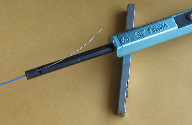
I have a web page answering WW questions and doubts, at http://wilsonminesco.com/6502primer/WireWrap.html . I use the OK Industries WSU 30-M tool shown here
which I expect is still available at lots of distributors. As WW has lost the economy of scale in recent years, the price of sockets has particularly become a bit of a monster, and to a lesser extent, the wire has. The tool is something you only buy once, so I'm not so concerned there. WW allows you to get the sockets shoulder to shoulder across the board, minimizing connection length so the AC behavior is better, unlike a two-layer PCB which needs room between sockets to route enough traces. A WW board can also be added onto or modified later. It was definitely king before the prices of PCBs came way down. There is perfboard available with a ground plane. Twin Industries' index to them is here. They also have perfboard with a plane on each side, here. These both have plated-thru holes.
The only reason I mentioned a power plane is that PCBWay seems to have even numbered layer options, so to have 3, I need 4. As a layout convenience, having a net that everything on the board needs access to sounds convenient, and power seems to be the obvious use for the extra layer.
Since I do have the thing running well on a breadboard, I figure its gonna be hard to come up with a PCB that doesn't work.
If you go for a 4-layer board, having only one plane (a ground plane) leaves you with three signal layers which might make for much easier routing and higher density than two signal layers would. If you get in a bind, rather than adding another pair of layers to get a few last traces in, there may not be anything wrong with having jumper wires that hug the board's surface on one side or the other. There used to be lots of these (although they were short, bare ones) in audio consumer electronics before double-sided boards with plated-thru holes were pretty standard.
If you go for a 4-layer board, having only one plane (a ground plane) leaves you with three signal layers which might make for much easier routing and higher density than two signal layers would.
However, having an inner power plane as well as ground plane makes the two act as an oversized bypass capacitor, which further helps with noise control. Also, power distribution no longer takes up part of an outer layer, which allows you to tighten density.
The following is not something that hobbyists would use, but interesting nevertheless. I have in front of me a 45-page book on Zycon's BC (buried capacitance) PCB technology from the mid-1990's. What they do is put the power and ground planes extremely close together to increase the capacitance between them—so close they ask you what the power supply voltage will be, which I assume (without re-reading the book) is so they don't give you something that will get punched through if you use 5V on a board meant for 3.3V. They get over 500pF per square inch. Multiple (four) power and ground plane pairs have been used in 16-layer boards to get over 2,000pF per square inch, or .002uF/in². That's still not a lot, but if you're trying to get the board to pass a stringent radiation emission requirements test, it can help, my eliminating the inductance of the short traces needed to connect decoupling capacitors which you'll no longer need. It says it's generally for edge rates below 10ns and clock rates above 25MHz, and that in those cases, you can usually get rid of all the discrete decoupling capacitors. I considered using it for a product back then, but then the project got canceled. [Edit, June 2022: After listening to lectures from some experts in the field, I realize now that a problem with the signal-ground-power-signal typical PCB stackup is that the power and ground layers are the two layers that are farthest apart, and if you have a via to take a signal from layer 1 to layer 4, its return current has to go quite a ways out from that via, causing signal-integrity problems. The BC technology mentioned above, with its high amount of capacitance per square centimeter, helps the return current stay close to be via and solve the problem; so it's not just about keeping the power supply quiet.]
I'd be surprised if the capacitance between the inner planes of a regular 4-layer board was a useful amount - for example, if it allowed one to use fewer bypass caps with confidence. Do you have the numbers BDD?
The dielectric constant of FR4 board is approximately 4.1, and you can use that in the capacitor equation
C=.2235*KA/d*(N-1)
where C is the capacitance in pF,
K is the dielectric constant (4.1 in this case),
A is the area of one plate in square inches,
d in the thickness of the dielectric in inches, and
N is the number of plates.
So for a 4-layer, .062"-thick board with the layers evenly spaced and the inner layers being the planes at .020" apart, you get
.2235 * 4.1 * 1 / .020 * (2-1) = 46pF for one square inch, less than a tenth as much as the Zycon BC technology (which still wasn't monumental).
A nice thing, as I remember from one of Dr. Howard Johnson's articles on high-speed digital design, is that parallel planes close to each other have no inductance (as long as you stay far enough away from the edges to approximate an infinite plane), so it the board has enough capacitance in chip capacitors, you don't need a capacitor right next to every IC. You can put them wherever they fit best, even if it's kind of far from some ICs.
I'd be surprised if the capacitance between the inner planes of a regular 4-layer board was a useful amount - for example, if it allowed one to use fewer bypass caps with confidence. Do you have the numbers BDD?
Garth beat me to it.
As an example, POC V1.1 has a 21.00 square inch board. Using the 46 pF per square inch number Garth calculated the "capacitor" formed by the inner layers would be 966 pF. POC V2.1's board is slightly larger at 22.56 square inches, producing approximately 1038 pF (0.001 µF). It's not a lot but it does help.
GARTHWILSON wrote:
A nice thing, as I remember from one of Dr. Howard Johnson's articles on high-speed digital design, is that parallel planes close to each other have no inductance (as long as you stay far enough away from the edges to approximate an infinite plane), so it the board has enough capacitance in chip capacitors, you don't need a capacitor right next to every IC. You can put them wherever they fit best, even if it's kind of far from some ICs.
This is the less obvious benefit of the internal power and ground planes. Also, ground bounce is much less a problem and voltage distribution to everything wired to Vcc is much more even.
totally stupid question considering how far along I am.
Should the PHI2 pin on my ACIA be hooked to the PHI2O on the MPU, or directly to the oscillator output.
I'm doing the actual schematic so I can do a board, and noticed my ACIA's PHI2 is coming right from the the oscillator. I tried hooking it to the PHI2O on the MPU, and got crashes.
Makes me wonder exactly what the difference is anyway. It almost kinda worked.
Also, I don't currently have the IRQ pin on my 6522 hooked up (wasn't using it)
I remember reading somewhere that if I do want to use it, and I have other devices using the IRQ line, I need an AND gate or something or I'll get conflicts. Can't find where I read this, but I'm sure I did. Only other device that currently uses the IRQ line is the ACIA.