Issue with Indirect Addressing
Re: Issue with Indirect Addressing
Sure i will create one now, I have the CS for RAM tied with the Rising edge of Phase 2 out (from what i saw this is correct). This is the same for both Video RAM as well as system RAM, whats weird about it is that as i monitor the lines on a very slow clock rate there is not even a write that gets issued during the indirect addressing - only after when it stores the value of 00 in video ram.
-
barrym95838

- Posts: 2056
- Joined: 30 Jun 2013
- Location: Sacramento, CA, USA
Re: Issue with Indirect Addressing
Hi ChaseHQ85,
I'm at work right now, but when I get home I would like to supply you with a re-written version of your code for testing purposes, based on what I think you're trying to do with yours. I want to encourage you to learn efficient coding habits, and the best way to do that is to jump in and post your code for review, but hand-simulating your source is making me grind my teeth too much.
Mike B.

Re: Issue with Indirect Addressing
I'm thinking the trouble could be at the very end of the cycle where the high byte is read: the next cycle is a write, and if that write signal is applied when the RAM is still accessing the high byte, it will write instead of reading. But it doesn't quite hang together. Indeed, for an indexed write I think there might be another read cycle in between.
I think it's a big clue, if you're getting a write back into zero page.
I think it's a big clue, if you're getting a write back into zero page.
Re: Issue with Indirect Addressing
Mike and Ed! Thank you so much for your assistance! Id be more than happy to run a revision of the code. I will continue to investigate a write back at the wrong time, as I go through it, it seems correct but i may of definitely over looked something so i will do that look over now.
Thanks!
Thanks!
Re: Issue with Indirect Addressing
An Update! So after BigEd suggestion of it having to do with WR timing, I decided to remove my NAND gate from Phase2 out and CS and viola it all works as expected. Which is weird because that goes against timing. Here is what i think it is - and please correct me if im completely wrong.
So... My high performance low propagation time NAND gates are coming in tomorrow, so until then I created a NAND gate out of two 2n2222 transistors - I cannot find any propagation or switch time in any datasheet for them but apparently they could be the source of why the timing was off. I wont be able to confirm this until the correct Gates come in the mail tomorrow. Until then, just driving the CS off my decoding logic seems to work just fine... for now im sure... while there is nothing crazy going on or any high clock frequency.
Let me know your thoughts, but i am ecstatic that it's working.
-
BigDumbDinosaur

- Posts: 9428
- Joined: 28 May 2009
- Location: Midwestern USA (JB Pritzker’s dystopia)
- Contact:
Re: Issue with Indirect Addressing
ChaseHQ85 wrote:
An Update! So after BigEd suggestion of it having to do with WR timing, I decided to remove my NAND gate from Phase2 out and CS and viola it all works as expected. Which is weird because that goes against timing. Here is what i think it is - and please correct me if im completely wrong.
So... My high performance low propagation time NAND gates are coming in tomorrow, so until then I created a NAND gate out of two 2n2222 transistors - I cannot find any propagation or switch time in any datasheet for them but apparently they could be the source of why the timing was off. I wont be able to confirm this until the correct Gates come in the mail tomorrow. Until then, just driving the CS off my decoding logic seems to work just fine... for now im sure... while there is nothing crazy going on or any high clock frequency.
Let me know your thoughts, but i am ecstatic that it's working.
So... My high performance low propagation time NAND gates are coming in tomorrow, so until then I created a NAND gate out of two 2n2222 transistors - I cannot find any propagation or switch time in any datasheet for them but apparently they could be the source of why the timing was off. I wont be able to confirm this until the correct Gates come in the mail tomorrow. Until then, just driving the CS off my decoding logic seems to work just fine... for now im sure... while there is nothing crazy going on or any high clock frequency.
Let me know your thoughts, but i am ecstatic that it's working.
Regarding SRAM control, I know Garth's primer shows a circuit in which /CS is qualified by Ø2. The problem with doing it that way is you lose part of Ø2 low when you could be doing your setup. You should gate /CS as soon as a valid address is on the bus, which occurs approximately midway during Ø2 low on the 65C02 and 65C816.
What does need to be qualified by Ø2 is RWB, as allowing a write when Ø2 is low can have undefined effects, especially when access I/O hardware. The data bus contains undefined content during Ø2 low. Qualifying reads and writes with Ø2 addresses that matter. See attached for an example circuit.
- Attachments
-
- Read/Write Circuit
Last edited by BigDumbDinosaur on Wed Feb 22, 2017 4:57 am, edited 1 time in total.
x86? We ain't got no x86. We don't NEED no stinking x86!
Re: Issue with Indirect Addressing
BigDumbDinosaur wrote:
ChaseHQ85 wrote:
BigEd wrote:
Could you swap out the CPU? Just in case...
The program ended up working out after removing the NAND gate from Phase 2 out and RAM CS - I suspect it is because im using 2x 2n2222's as a NAND gate. I can further test that tomorrow when my highspeed low propagation 74 series logic gates arrive. Until then im trying to find out some type of documentation on 2n2222 delay's.
Thanks for the post!
-
GARTHWILSON

- Forum Moderator
- Posts: 8775
- Joined: 30 Aug 2002
- Location: Southern California
- Contact:
Re: Issue with Indirect Addressing
BigDumbDinosaur wrote:
Regarding SRAM control, I know Garth's primer shows a circuit in which /CS is qualified by Ø2. The problem with doing it that way is you lose part of Ø2 low when you could be doing your setup. You should gate /CS as soon as a valid address is on the bus, which occurs approximately midway during Ø2 low on the 65C02 and 65C816.
Quote:
What does need to be qualified by Ø2 is RWB, as allowing a write when Ø2 is low can have undefined effects, especially when access I/O hardware. The data bus contains undefined content during Ø2 low. Qualifying reads and writes with Ø2 addresses that matter. See attached for an example circuit.
http://WilsonMinesCo.com/ lots of 6502 resources
The "second front page" is http://wilsonminesco.com/links.html .
What's an additional VIA among friends, anyhow?
The "second front page" is http://wilsonminesco.com/links.html .
What's an additional VIA among friends, anyhow?
Re: Issue with Indirect Addressing
Quote:
Let me know your thoughts, but i am ecstatic that it's working.
(About bad silicon: the last time I saw it was with 933MHz Pentium machines from IBM. We had 50-100 of them running chip simulation jobs. After much debugging of a stray simulation error, we found one of them would make one very specific error when running a simulation. For all other purposes, it was fine. We took that machine offline. In an earlier generation, when SPARC was king, I know the people at Sun -would automatically re-run any chip simulation which failed. Only the second failure counted. So, at modest scale, you might come across a microprocessor with an internal flaw. But it's a good principle not to make this your first hypothesis - I think many programmers go through a phase of blaming the compiler, because sometimes compilers have bugs, but the far more frequent case is that the program has a bug.)
-
barrym95838
- Posts: 2056
- Joined: 30 Jun 2013
- Location: Sacramento, CA, USA
Re: Issue with Indirect Addressing
Hello again, ChaseHQ85. I'm glad to see that you found your problem. I'm providing an untested re-write of your source, in the hopes of showing you a different way of attacking the specific task you posted. I think that I understood what you were doing with your code, with the exception of your mention of the number "2820" in your comments. 
When it is possible to do so, it can be of benefit to fill from higher to lower addresses on the 65xx, especially if the fill area is not an integer multiple of 256, and this is the technique I have employed here. The accumulator and Y register don't have to be initialized inside the loops, because they already have the "correct" value when the loop-backs occur. Not only is the static instruction count lower, but the nested loops execute far fewer instructions, with the net result being a more efficient system.
If I messed up anywhere, please let me know, and I'll revise.
Mike B.
When it is possible to do so, it can be of benefit to fill from higher to lower addresses on the 65xx, especially if the fill area is not an integer multiple of 256, and this is the technique I have employed here. The accumulator and Y register don't have to be initialized inside the loops, because they already have the "correct" value when the loop-backs occur. Not only is the static instruction count lower, but the nested loops execute far fewer instructions, with the net result being a more efficient system.
Code: Select all
   PROCESSOR 6502

;-------------------------------------------------
;-------------DANI-I-SYSTEM-ROM-------------------
;-------------------------------------------------

;-------------EQUATES-----------------------------
VRAM:            EQU $8000
VRAM_H:          EQU $80
VRAM_L:          EQU $00
VRAM_CMD:        EQU VRAM + $F00
VRAM_CHARSLOC:   EQU VRAM + $F10
VRAM_CHARSBUF:   EQU VRAM + $F20
;-------------EO-EQUATES--------------------------

    ORG $C000
RESET:
    LDX #$FF            ; Initialize the Stack Pointer
    TXS                 ; Transfer X to Stack
SETUP_BLANKCHAR:
    LDA #$00            ; Store Null in Accu
    LDX #$07            ; Set X to 7
LOOP_BLANKSTORE:
    STA VRAM_CHARSBUF,X ; Store Accu into VRAM_CHARSBUF+X
    DEX                 ; (filling high to low is more efficient)
    BPL LOOP_BLANKSTORE
    STA VRAM_CHARSLOC   ; Set the Character Store Location
    LDA #$01            ; Set the Character Store Command
    STA VRAM_CMD
CHECK_CMDCOMPLETE:
    LDA VRAM_CMD        ; Check VRAM_CMD to see if VGA picked up char
    BNE CHECK_CMDCOMPLETE ; Keep checking until it resets to 00
BLANKOUT_START:
    LDA #VRAM_L         ; Load Low Byte of VRAM address
    STA $05             ; Store it in Zero Page 5
    LDY #$B0            ; Last page is only partially filled
    LDA #$00            ; Set Accu To 0 (fill byte)
    LDX #VRAM_H+4       ; Init X to last VRAM page number
LOOP_BL_OUTER:
      STX $06           ; Store it in Zero Page 6
LOOP_BL_INNER:
        DEY             ; (filling high to low is more efficient)
        STA ($05),Y     ; Store the fill byte
        BNE LOOP_BL_INNER ; ... down to the bottom of the page
      DEX               ; Prepare to fill next-lower page
      CPX #VRAM_H       ; Is X < VRAM_H?
      BCS LOOP_BL_OUTER ; No: fill the next page
LOOP_DONE:
    JMP LOOP_DONE       ; Done: "halt" in an infinite loop
VECTORS:
    ORG $FFFA           ; 6502 Starts reading its vectors here
    .word LOOP_DONE     ; NMI
    .word RESET         ; RESET
    .word LOOP_DONE     ; BRK

   END
Mike B.
Re: Issue with Indirect Addressing
barrym95838 wrote:
Hello again, ChaseHQ85. I'm glad to see that you found your problem. I'm providing an untested re-write of your source, in the hopes of showing you a different way of attacking the specific task you posted. I think that I understood what you were doing with your code, with the exception of your mention of the number "2820" in your comments.
When it is possible to do so, it can be of benefit to fill from higher to lower addresses on the 65xx, especially if the fill area is not an integer multiple of 256, and this is the technique I have employed here. The accumulator and Y register don't have to be initialized inside the loops, because they already have the "correct" value when the loop-backs occur. Not only is the static instruction count lower, but the nested loops execute far fewer instructions, with the net result being a more efficient system.
If I messed up anywhere, please let me know, and I'll revise.
Mike B.
When it is possible to do so, it can be of benefit to fill from higher to lower addresses on the 65xx, especially if the fill area is not an integer multiple of 256, and this is the technique I have employed here. The accumulator and Y register don't have to be initialized inside the loops, because they already have the "correct" value when the loop-backs occur. Not only is the static instruction count lower, but the nested loops execute far fewer instructions, with the net result being a more efficient system.
Code: Select all
   PROCESSOR 6502

;-------------------------------------------------
;-------------DANI-I-SYSTEM-ROM-------------------
;-------------------------------------------------

;-------------EQUATES-----------------------------
VRAM:            EQU $8000
VRAM_H:          EQU $80
VRAM_L:          EQU $00
VRAM_CMD:        EQU VRAM + $F00
VRAM_CHARSLOC:   EQU VRAM + $F10
VRAM_CHARSBUF:   EQU VRAM + $F20
;-------------EO-EQUATES--------------------------

    ORG $C000
RESET:
    LDX #$FF            ; Initialize the Stack Pointer
    TXS                 ; Transfer X to Stack
SETUP_BLANKCHAR:
    LDA #$00            ; Store Null in Accu
    LDX #$07            ; Set X to 7
LOOP_BLANKSTORE:
    STA VRAM_CHARSBUF,X ; Store Accu into VRAM_CHARSBUF+X
    DEX                 ; (filling high to low is more efficient)
    BPL LOOP_BLANKSTORE
    STA VRAM_CHARSLOC   ; Set the Character Store Location
    LDA #$01            ; Set the Character Store Command
    STA VRAM_CMD
CHECK_CMDCOMPLETE:
    LDA VRAM_CMD        ; Check VRAM_CMD to see if VGA picked up char
    BNE CHECK_CMDCOMPLETE ; Keep checking until it resets to 00
BLANKOUT_START:
    LDA #VRAM_L         ; Load Low Byte of VRAM address
    STA $05             ; Store it in Zero Page 5
    LDY #$B0            ; Last page is only partially filled
    LDA #$00            ; Set Accu To 0 (fill byte)
    LDX #VRAM_H+4       ; Init X to last VRAM page number
LOOP_BL_OUTER:
      STX $06           ; Store it in Zero Page 6
LOOP_BL_INNER:
        DEY             ; (filling high to low is more efficient)
        STA ($05),Y     ; Store the fill byte
        BNE LOOP_BL_INNER ; ... down to the bottom of the page
      DEX               ; Prepare to fill next-lower page
      CPX #VRAM_H       ; Is X < VRAM_H?
      BCS LOOP_BL_OUTER ; No: fill the next page
LOOP_DONE:
    JMP LOOP_DONE       ; Done: "halt" in an infinite loop
VECTORS:
    ORG $FFFA           ; 6502 Starts reading its vectors here
    .word LOOP_DONE     ; NMI
    .word RESET         ; RESET
    .word LOOP_DONE     ; BRK

   END
Mike B.
Re: Issue with Indirect Addressing
It would be great if some time you can share the story of your build, with description and photos!
If you're staying - and I hope you are - perhaps you could post in the Introduce Yourself thread.
If you're staying - and I hope you are - perhaps you could post in the Introduce Yourself thread.
Re: Issue with Indirect Addressing
BigEd wrote:
It would be great if some time you can share the story of your build, with description and photos!
If you're staying - and I hope you are - perhaps you could post in the Introduce Yourself thread.
If you're staying - and I hope you are - perhaps you could post in the Introduce Yourself thread.

Re: Issue with Indirect Addressing
ChaseHQ85 wrote:
I created a NAND gate out of two 2n2222 transistors
-- Jeff
- Attachments
-
- gates.png (3.47 KiB) Viewed 1051 times
In 1988 my 65C02 got six new registers and 44 new full-speed instructions!
https://laughtonelectronics.com/Arcana/ ... mmary.html
https://laughtonelectronics.com/Arcana/ ... mmary.html
Re: Issue with Indirect Addressing
Hey Jeff,
This is the NAND gate I used.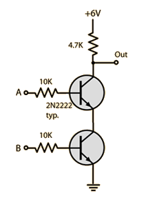
But... Great News!~ The logic gates arrived, i plugged them in, and up to 4mhz on a breadboard so far with zero issues! I couldn't get it over 350khz prior with the transistor setup. I have the RAM and VRAM set up that writes are only valid on rising edge of clock now as well. Safe to say, im on my way! I'll keep you all posted!