Vulcan-74 - A 6502 Powered Retro MegaProject
- Oneironaut
- Posts: 734
- Joined: 25 May 2015
- Location: Gillies, Ontario, Canada
- Contact:
Re: Vulcan-74 - A 6502 Compatible Retro MegaProject
Well, Old Man Winter has moved back in around here, so I will have a few hours per week again to work on Vulcan-74.
Yesterday, I managed to get test a few of my latest design ideas, and now have direction.
The 8 into 24 bit palette idea failed.
Having the SRAM lookup table in the path of the video output simply added too much propagation delay.
The video did work, but I was violating the setup times of the last 74HC574 by 5 nanoseconds.
For this reason, I decided to scrap the idea.
The good news is that the 16 bit data bus was a total success, so Vulcan now handles 12 bit color natively.
So now I can display 4096 colors fully, rather than only 256 (if using a palette lookup table).
Sprites and bitmaps will also be stored as true 4096 color images.
This proves my initial idea of using 12 bits out of 16 to store graphics, and utilizing the spare bits for special functions.
This design will also speed up the Sprite Generator by using a dedicated alpha color bit and X counter wrap bit.
The downside to using a full 16 bit data bus is of course the need to double up on all SRAM (12 x 512K SRAMs required now).
If I could find a cost effective source for 25 of these, then it would be no issue...
http://www.proto-advantage.com/store/pr ... id=2200247
Might just make my own boards. The I could use 256Kx16 TSOP rather than 512Kx8 SOJ packages.
Currently, I have the new 16 bit data bus wired up, and have random pixels outputting from the dual buffer Video Memory.
The initial test will be to connect my AVR to stuff an image into the back buffer to test the Video Generator.
Sprites should look great in 4096 colors as compared to my original uneven 8 bit color space.
In the old design, I used 8 bits as RRR-GGG-BB, and now I am using 13 bits as RRRR-GGGG-BBBB-A (A = invisible Alpha color).
With a dedicated Alpha Bit, the Sprite Generator no longer requires the comparator, so the hardware will be much faster as well.
At this point, I am not sure about mixing the Sprite Memory with the Playfield Memory. It will depend on the final hardware speed.
I will post a few videos once the 4096 color Video Generator has an image up on the screen.
Cheers,
Radical Brad
Re: Vulcan-74 - A 6502 Compatible Retro MegaProject
Quote:
Having the SRAM lookup table in the path of the video output simply added too much propagation delay.
- Oneironaut
- Posts: 734
- Joined: 25 May 2015
- Location: Gillies, Ontario, Canada
- Contact:
Re: Vulcan-74 - A 6502 Compatible Retro MegaProject
Nope.
The best case scenario (old design) was : 574(16) + 688(20) + 7404(8) + 574(16) = 60ns
This is using "typical" ratings on "typical" 74HC logic, which is all I am allowing myself.
With this design, I managed a top Sprite bandwidth of 5Mhz.
Another consideration is the way the X/Y counter box comparators used to work.
In my new design, there is no delay at all since the Alpha Bit is dedicated.
Even considering a margin of error, I expect to easily hit 10Mhz, possibly 16Mhz.
Gaining 60ns seems like nothing, but considering a 32x32 sprite, performance will go from 50 sprites to 200 easily!
Another benefit is the 4096 colors, which means edge aliasing will be almost unnoticeable.
400x300 with 4096 colors will look better than 640x480 with 256 colors by far.
Brad
Couldn't you add a register stage ?
The best case scenario (old design) was : 574(16) + 688(20) + 7404(8) + 574(16) = 60ns
This is using "typical" ratings on "typical" 74HC logic, which is all I am allowing myself.
With this design, I managed a top Sprite bandwidth of 5Mhz.
Another consideration is the way the X/Y counter box comparators used to work.
In my new design, there is no delay at all since the Alpha Bit is dedicated.
Even considering a margin of error, I expect to easily hit 10Mhz, possibly 16Mhz.
Gaining 60ns seems like nothing, but considering a 32x32 sprite, performance will go from 50 sprites to 200 easily!
Another benefit is the 4096 colors, which means edge aliasing will be almost unnoticeable.
400x300 with 4096 colors will look better than 640x480 with 256 colors by far.
Brad
Arlet wrote:
Quote:
Having the SRAM lookup table in the path of the video output simply added too much propagation delay.
- Oneironaut
- Posts: 734
- Joined: 25 May 2015
- Location: Gillies, Ontario, Canada
- Contact:
Re: Vulcan-74 - A 6502 Compatible Retro MegaProject
Vulcan-6502 Reloaded has now become real.
I had a full day to test some of the new design ideas, and so far everything has worked as planned.
Choosing to go from 8 colors to 4096 colors required the data bus to grow from 8 bits to 16 bits all the way around.
There are 2 ways to get a 16 bit SRAM : using actual 16 bit SRAM, or by doubling up on 8 bit SRAM. I chose the later.
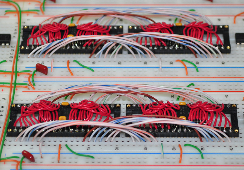
A series / parallel configuration to create a 1MB x 16 SRAM.
SRAM can be connected with the data bus in series or parallel to create just about any configuration.
Four 256K x 16 SRAMs make up a 1MB x 16 memory when their CE lines are tied together with a 2-4 decoder.
In my case, I paralleled the address busses on two 512K SRAMs, and then used their data ports in series.
I then tied their CE lines with an inverter so that I had a 20 bit address bus and a 16 bit data bus (1MB x 16).
I would have purchased new 256K x 16 SRAM is I didn't already have a full tray of 10ns 512K x 8 SRAMs available.
In the end, both methods offer the same result anyhow. Actually, there are benefits to using the 512K x 8 SRAMs.
Going to 16 bits from 8 bits was a huge change to the entire board, which is why I started from the beginning.
Even the final output to the resitor DAC had to fatten up, as color uses 12 of the 16 available bits.
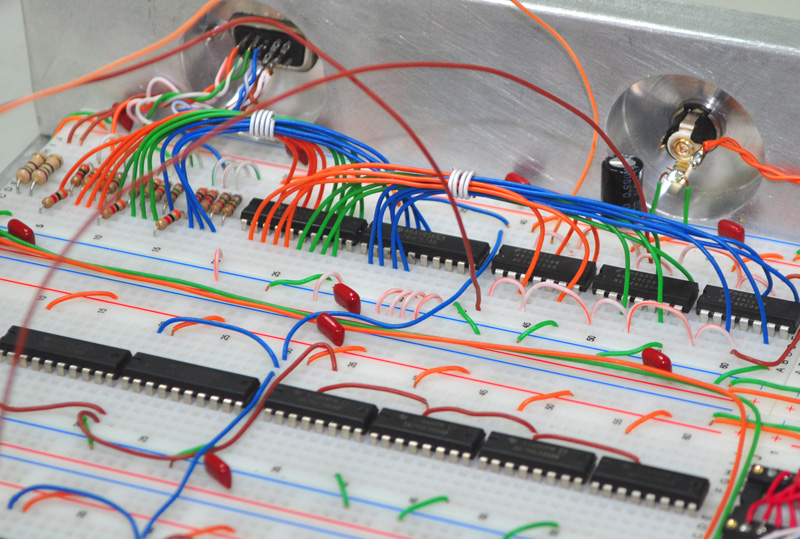
For 12 bit of color (4096 colors), the number of latches and buffers must double.
The new 12+1 bit color space is RRRR-GGGG-BBBB-A, which means 4 bits for each primary color, and 1 bit for invisible pixels.
In the original design, the 8 bit color space was just RRR-GGG-BB, so a single 74HC574 or 74HC245 could handle the bus.
Now I will require double the number of ICs to pass the data bus around, and 12 resistors for the DAC rather than just 8.
The photo above shows the color bits as being Red, Green and Blue wires.
To "sync" up the blanking time with the pixel clock, color bits are ANDed with the pixel clock using the 74HC08 AND gates.
After syncing the bits through the AND gates, they are then driven out to the DAC through the two 74HC574 registers.
This system has worked perfectly in all previous designs as well. Even a 1ns delay between blanking and pixel is highly noticeable on the screen!
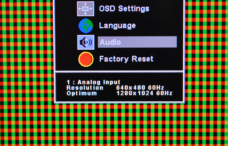
Testing the new DAC and timing on the monitor.
After doing some successful testing with 640x480 resolution, I decided that 400x300 resolution was better for a game system.
The main goal is to deliver high speed Sprites and Images, and at 640x480, the number of pixels per screen is so much larger.
Although the VGA Generator worked perfectly at 640x480, the amount of SRAM required was huge, and the frame rate was much lower.
Now that I have 4096 colors instead of only 256, the image quality will stlll be much better, so I settled back to 400x300 resolution.
As shown above, the monitor had no problems with 640x480, although I would say this is the upper limit for 74HC logic!
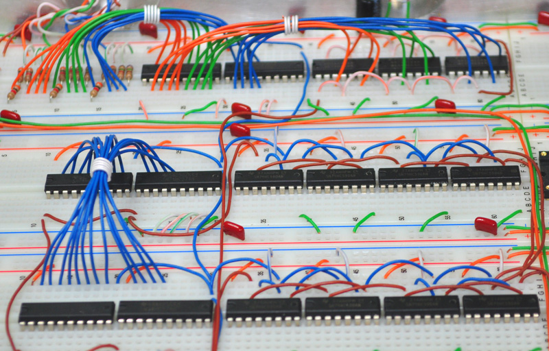
In the new design, the X/Y counters are cloned 3 times.
Another huge design change I made was in the way that the Sprite Generator and VGA Generator share access to the Video Memory.
Video Memory consists of 2 swappable banks. One is being drawn to screen while the other is accessible by the GPU hardware.
In the previous design, the VGA Generator and GPU fed into a large bank of 74HC245s that created a massive bus switcher.
One set of 245s drove the 20 bit address bus and 8 bit data bus to the Live Buffer with the other drove the Back Buffer.
This certainly worked well, but the resulting pathway had an extra 10 nanoseconds of travel to make it through the gates.
in the new design, I realized that I didn't actually need any of the 245s, as I could just make use of the OE function on the counters.
So now I have 3 sets of X/Y counters, each of them synced together from the master 20MHz Pixel Clock.
Here is how this works...
Counter Set One : Drives the 74HC688 comparators in order to generate the Video Signals. Counters are tapped so that they divide by 4.
Counter Set Two : Drives Video Bank One directly so that when this bank is "Live", it is drawn to the screen.
Counter Set Three : A mirror image of Counter Set Two. Only one can be active at any time. The other is disabled by OE (tristated).
So when one of the Pixel Driving Counter Sets is disabled, the GPU gets access to that Video Bank, since it is now the "Back Buffer".
Having shaved about 10ns of the path means that I can push the Sprite Generator up even more when I get started on the design.
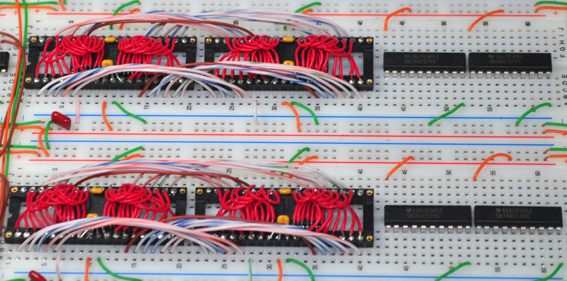
The Data Bus Switch is now 16 Bits Wide.
The Data Bus Switch is also double the width. These are just 74HC574s that feed into the Video memory Banks.
Although the system would be capable of displaying true 16 bit color, I am only using 12 bits for color.
The other 4 bits are used internally to speed up the Sprite Generator. I guess they could be considered "micro-code".
Here is how all 16 bits are going to be used in the new design...
In the old design, the Alpha Color was detected by feeding the Data Bus to a 74HC688 comparator, which then fed an inverter, FlipFlop.
Alpha Detection was the bottleneck in the old Sprite Generator, and now there is no delay at all!
The X/Y box logic in the Sprite Generator will also be driven by the special bits, so it will also run at maximum speed.
I am hoping to get 10MHz out of the new Sprite Generator, which will by a 3x speed increase over the previous version.
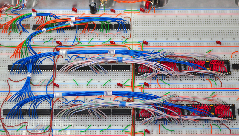
Connecting the Counter Chains to the Video Memory.
One of the most time consuming aspects of bread-boarding a 16 bit, high speed Video Game System is... so many wires!
In the photo above, I have connected the switchable address counters to the double Video Memory Banks.
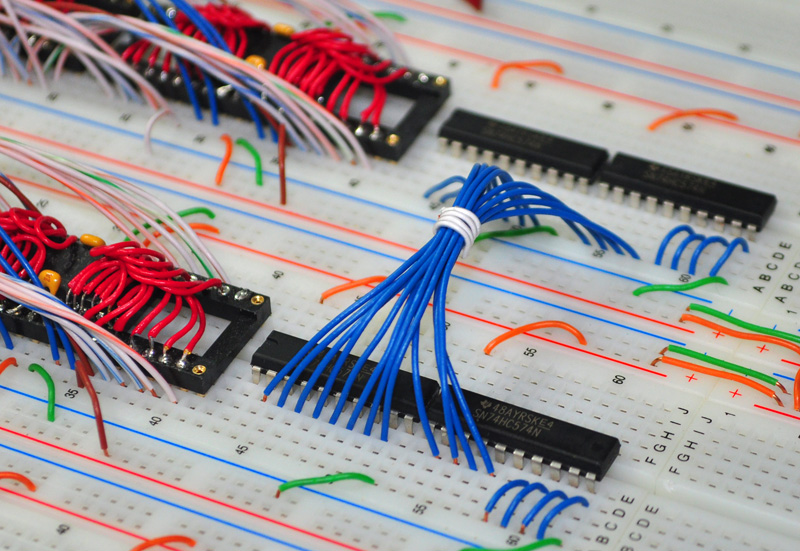
Connecting the Data Bus Switches to the Video Memory.
When the counters to the left of the SRAM are active, the 74HC574s to the right are disabled, and the opposite is true for the other bank.
The photo above shows the 12 Data Lines that feed into the Video Memory Bus Switch.
Only 12 bits ever reach the Video Memory, since the other 4 special bits are used internally by the Sprite Generator.
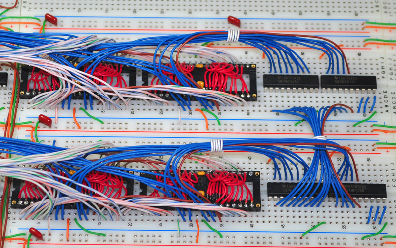
The completed Dual 12 Bit Switchable Data Bus.
As you can see, I always use Blue wires for Data Lines, and White wires for Address Lines.
Brown wires are control lines, and the VCC and Ground connections are Red and Green.
The single Brown wire shown heading into the Bus Switch controls the SRAM Write Enable Line.
I feed this through the 574 chain so that WE is registered in sync with any data to be written to the back buffer.
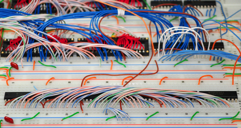
Adding a Switchable 18 Bit Address Bus.
The six 74HC574s shown above will create a switchable 18 bit address bus into the double buffered Video Memory.
The address is split into X (9 Bits) and Y (9 Bits), since the addressable box is 400 x 300 pixels.
Just like the 574s the swap the Data Bus, these 574s do the same with the incoming Address Bus from the GPU.
This switch works along with the Counter Switch, making sure only opposing sets are active.
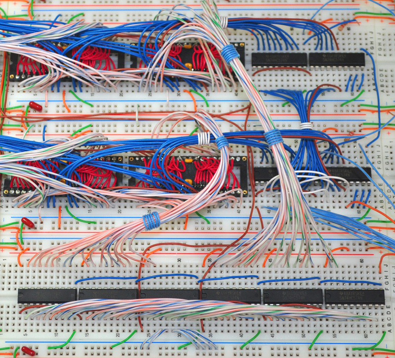
The Complete Address and Data Switch into the Video memory.
Did I mention that this type of prototyping requires a LOT of wires??
I cut every single wire to the required length by hand, and then bend them into shape for a neater appearance.
Does it really matter if the final wiring looks neat?... it does to me!
Perhaps this careful planning of wiring is why my breadboard can run reliably up to 32MHz? Who knows!
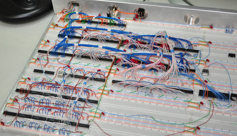
The New 4096 Color Video Generator is now ready for testing..
The only part of the entire design that remains original are the bottom left 2 rows of X/Y comparators.
Everything else is completely redone, and rewired from scratch.
The photo above shows the bare-bones VGA Generator along with the input switch that the GPU will connect to.
For testing, I put my 6502 simulator (AVR 1284) back on the board and loaded it with a 12 bit image.
The AVR pretends to be a 6502 by emulating the address, data, and RW lines of a 6502.
Using the AVR for testing is nice because I can directly load it from the PC, and it has 128K of internal EEPROM space.
Now that an image takes up twice the memory, I cannot even hold a full 400x300 image, as this would require 240K of space.
Later, this will not be an issue, as the external "Cartridge" will be capable of megabytes of data.
Now for some real image testing. At this point, I did not even know if the new 4096 color VGA Generator would work!
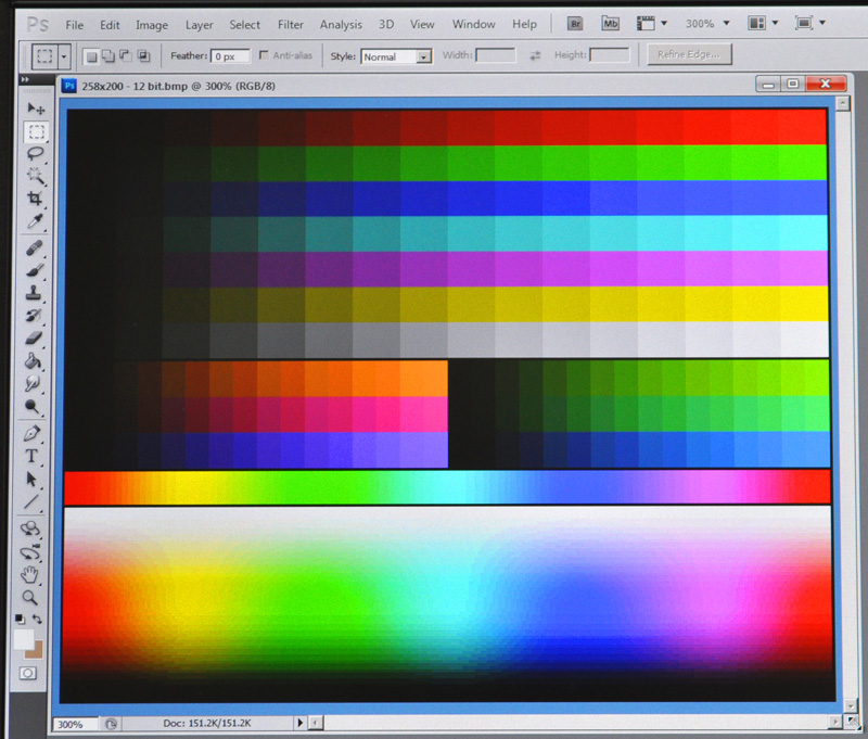
A 12 Bit Palette image to be used for testing.
I found a nice bitmap showing a 12 Bit Color Palette online, and saved it as a 300x200 image from Photoshop.
There as certainly a much richer variation of colors in the palette when compared to the limited 256 (8 bit) palette.
I also recoded my Sprite Converter Program to handle the conversion of 24 bits to 12 bits.
This program takes any Bitmap and then spites out assembly or C data that can be store in a micro-controller.
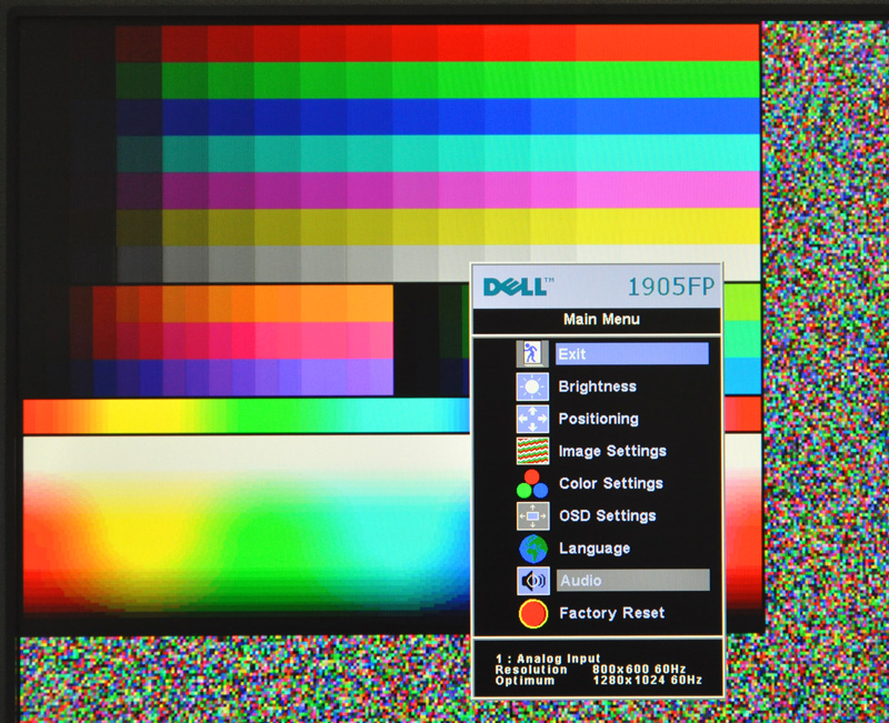
4096 Colors looking great on the new Vulcan-74 VGA Generator!
it was a pleasant surprise to see the new Video Generator come up for the first time and display an almost perfect representation!
The monitor reported 800x600, which is what my timing is generating, and the colors looked the same as on the original PC image.
The random pixels shown around the image are there because an SRAM contains random data when it is initially powered up.
Proof that 4096 colors could be displayed has now been confirmed!
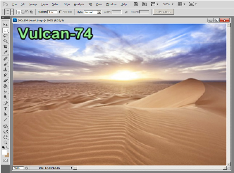
Another image to be converted and displayed.
The color palette looked so good that I needed to try a previous image so I could compare the difference.
The image above was displayed on the old version using only 256 colors, and it still looked pretty good.
Most of the small variations in color shades were lost though, and the image almost looked "posterized".
As you can see in the 24 bit original, the image is perfect as seen on the PC monitor.
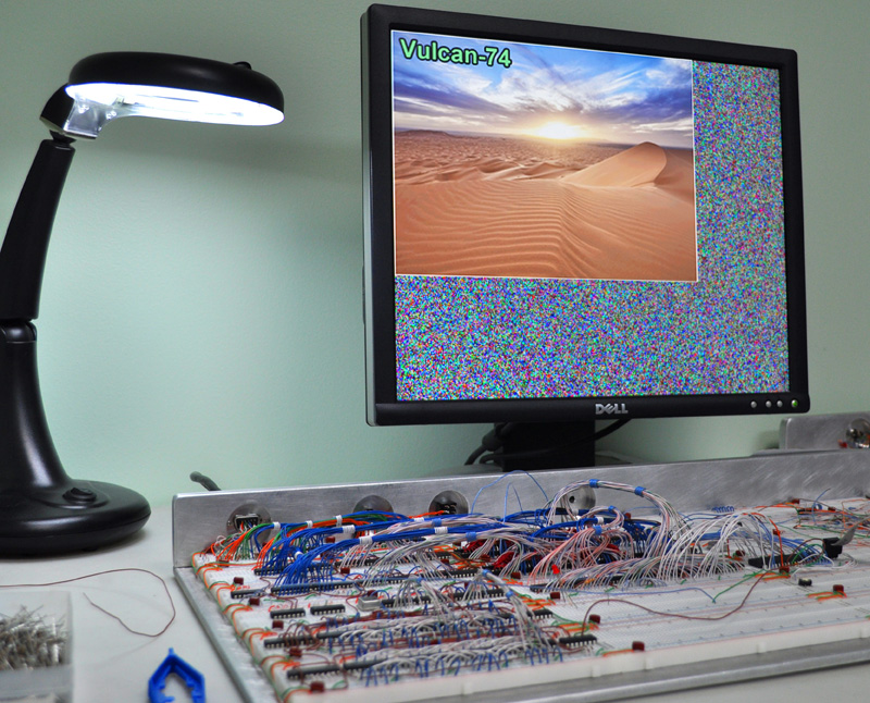
Vulcan-74 displaying a very clean 12 bit image.
When converted and loaded through the 6502 simulator, the resulting image looked great.
There is no comparison... 4096 colors blows 256 colors away by a huge margin.
The image being displayed on Vulcan-74 looks almost as good as it does on my PC monitor.
Not bad... 12 resistors doing the job of a $300 video card!
For my next test, I will be wiring up another 8 SRAMs in order to create a 2MB x 16 Sprite memory.
If I can get the Sprite Generator to run beyond 4MHz, then Vulcan-74 is going to have unreal power.
Even when it could only do 4MHz Sprites with 256 colors, it did a great job, so the new version is going to be insane.
The Sprite Generator is by far the most complex part of this project, so there will be many more photos coming.
I will report my progress... good or bad! So far it has been all good.
Cheers!
Radical Brad
I had a full day to test some of the new design ideas, and so far everything has worked as planned.
Choosing to go from 8 colors to 4096 colors required the data bus to grow from 8 bits to 16 bits all the way around.
There are 2 ways to get a 16 bit SRAM : using actual 16 bit SRAM, or by doubling up on 8 bit SRAM. I chose the later.

A series / parallel configuration to create a 1MB x 16 SRAM.
SRAM can be connected with the data bus in series or parallel to create just about any configuration.
Four 256K x 16 SRAMs make up a 1MB x 16 memory when their CE lines are tied together with a 2-4 decoder.
In my case, I paralleled the address busses on two 512K SRAMs, and then used their data ports in series.
I then tied their CE lines with an inverter so that I had a 20 bit address bus and a 16 bit data bus (1MB x 16).
I would have purchased new 256K x 16 SRAM is I didn't already have a full tray of 10ns 512K x 8 SRAMs available.
In the end, both methods offer the same result anyhow. Actually, there are benefits to using the 512K x 8 SRAMs.
Going to 16 bits from 8 bits was a huge change to the entire board, which is why I started from the beginning.
Even the final output to the resitor DAC had to fatten up, as color uses 12 of the 16 available bits.

For 12 bit of color (4096 colors), the number of latches and buffers must double.
The new 12+1 bit color space is RRRR-GGGG-BBBB-A, which means 4 bits for each primary color, and 1 bit for invisible pixels.
In the original design, the 8 bit color space was just RRR-GGG-BB, so a single 74HC574 or 74HC245 could handle the bus.
Now I will require double the number of ICs to pass the data bus around, and 12 resistors for the DAC rather than just 8.
The photo above shows the color bits as being Red, Green and Blue wires.
To "sync" up the blanking time with the pixel clock, color bits are ANDed with the pixel clock using the 74HC08 AND gates.
After syncing the bits through the AND gates, they are then driven out to the DAC through the two 74HC574 registers.
This system has worked perfectly in all previous designs as well. Even a 1ns delay between blanking and pixel is highly noticeable on the screen!

Testing the new DAC and timing on the monitor.
After doing some successful testing with 640x480 resolution, I decided that 400x300 resolution was better for a game system.
The main goal is to deliver high speed Sprites and Images, and at 640x480, the number of pixels per screen is so much larger.
Although the VGA Generator worked perfectly at 640x480, the amount of SRAM required was huge, and the frame rate was much lower.
Now that I have 4096 colors instead of only 256, the image quality will stlll be much better, so I settled back to 400x300 resolution.
As shown above, the monitor had no problems with 640x480, although I would say this is the upper limit for 74HC logic!

In the new design, the X/Y counters are cloned 3 times.
Another huge design change I made was in the way that the Sprite Generator and VGA Generator share access to the Video Memory.
Video Memory consists of 2 swappable banks. One is being drawn to screen while the other is accessible by the GPU hardware.
In the previous design, the VGA Generator and GPU fed into a large bank of 74HC245s that created a massive bus switcher.
One set of 245s drove the 20 bit address bus and 8 bit data bus to the Live Buffer with the other drove the Back Buffer.
This certainly worked well, but the resulting pathway had an extra 10 nanoseconds of travel to make it through the gates.
in the new design, I realized that I didn't actually need any of the 245s, as I could just make use of the OE function on the counters.
So now I have 3 sets of X/Y counters, each of them synced together from the master 20MHz Pixel Clock.
Here is how this works...
Counter Set One : Drives the 74HC688 comparators in order to generate the Video Signals. Counters are tapped so that they divide by 4.
Counter Set Two : Drives Video Bank One directly so that when this bank is "Live", it is drawn to the screen.
Counter Set Three : A mirror image of Counter Set Two. Only one can be active at any time. The other is disabled by OE (tristated).
So when one of the Pixel Driving Counter Sets is disabled, the GPU gets access to that Video Bank, since it is now the "Back Buffer".
Having shaved about 10ns of the path means that I can push the Sprite Generator up even more when I get started on the design.

The Data Bus Switch is now 16 Bits Wide.
The Data Bus Switch is also double the width. These are just 74HC574s that feed into the Video memory Banks.
Although the system would be capable of displaying true 16 bit color, I am only using 12 bits for color.
The other 4 bits are used internally to speed up the Sprite Generator. I guess they could be considered "micro-code".
Here is how all 16 bits are going to be used in the new design...
Code: Select all
Bit 00 : Red Color Bit 0
Bit 01 : Red Color Bit 1
Bit 02 : Red Color Bit 2
Bit 03 : Red Color Bit 3

Bit 04 : Green Color Bit 0
Bit 05 : Green Color Bit 1
Bit 06 : Green Color Bit 2
Bit 07 : Green Color Bit 3

Bit 08 : Blue Color Bit 0
Bit 09 : Blue Color Bit 1
Bit 10 : Blue Color Bit 2
Bit 11 : Blue Color Bit 3

Bit 12 : Alpha (Invisible) Pixel
Bit 13 : Wrap X Counter Logic
Bit 14 : End of Sprite Data
Bit 15 : Not Used
Alpha Detection was the bottleneck in the old Sprite Generator, and now there is no delay at all!
The X/Y box logic in the Sprite Generator will also be driven by the special bits, so it will also run at maximum speed.
I am hoping to get 10MHz out of the new Sprite Generator, which will by a 3x speed increase over the previous version.

Connecting the Counter Chains to the Video Memory.
One of the most time consuming aspects of bread-boarding a 16 bit, high speed Video Game System is... so many wires!
In the photo above, I have connected the switchable address counters to the double Video Memory Banks.

Connecting the Data Bus Switches to the Video Memory.
When the counters to the left of the SRAM are active, the 74HC574s to the right are disabled, and the opposite is true for the other bank.
The photo above shows the 12 Data Lines that feed into the Video Memory Bus Switch.
Only 12 bits ever reach the Video Memory, since the other 4 special bits are used internally by the Sprite Generator.

The completed Dual 12 Bit Switchable Data Bus.
As you can see, I always use Blue wires for Data Lines, and White wires for Address Lines.
Brown wires are control lines, and the VCC and Ground connections are Red and Green.
The single Brown wire shown heading into the Bus Switch controls the SRAM Write Enable Line.
I feed this through the 574 chain so that WE is registered in sync with any data to be written to the back buffer.

Adding a Switchable 18 Bit Address Bus.
The six 74HC574s shown above will create a switchable 18 bit address bus into the double buffered Video Memory.
The address is split into X (9 Bits) and Y (9 Bits), since the addressable box is 400 x 300 pixels.
Just like the 574s the swap the Data Bus, these 574s do the same with the incoming Address Bus from the GPU.
This switch works along with the Counter Switch, making sure only opposing sets are active.

The Complete Address and Data Switch into the Video memory.
Did I mention that this type of prototyping requires a LOT of wires??
I cut every single wire to the required length by hand, and then bend them into shape for a neater appearance.
Does it really matter if the final wiring looks neat?... it does to me!
Perhaps this careful planning of wiring is why my breadboard can run reliably up to 32MHz? Who knows!

The New 4096 Color Video Generator is now ready for testing..
The only part of the entire design that remains original are the bottom left 2 rows of X/Y comparators.
Everything else is completely redone, and rewired from scratch.
The photo above shows the bare-bones VGA Generator along with the input switch that the GPU will connect to.
For testing, I put my 6502 simulator (AVR 1284) back on the board and loaded it with a 12 bit image.
The AVR pretends to be a 6502 by emulating the address, data, and RW lines of a 6502.
Using the AVR for testing is nice because I can directly load it from the PC, and it has 128K of internal EEPROM space.
Now that an image takes up twice the memory, I cannot even hold a full 400x300 image, as this would require 240K of space.
Later, this will not be an issue, as the external "Cartridge" will be capable of megabytes of data.
Now for some real image testing. At this point, I did not even know if the new 4096 color VGA Generator would work!

A 12 Bit Palette image to be used for testing.
I found a nice bitmap showing a 12 Bit Color Palette online, and saved it as a 300x200 image from Photoshop.
There as certainly a much richer variation of colors in the palette when compared to the limited 256 (8 bit) palette.
I also recoded my Sprite Converter Program to handle the conversion of 24 bits to 12 bits.
This program takes any Bitmap and then spites out assembly or C data that can be store in a micro-controller.

4096 Colors looking great on the new Vulcan-74 VGA Generator!
it was a pleasant surprise to see the new Video Generator come up for the first time and display an almost perfect representation!
The monitor reported 800x600, which is what my timing is generating, and the colors looked the same as on the original PC image.
The random pixels shown around the image are there because an SRAM contains random data when it is initially powered up.
Proof that 4096 colors could be displayed has now been confirmed!

Another image to be converted and displayed.
The color palette looked so good that I needed to try a previous image so I could compare the difference.
The image above was displayed on the old version using only 256 colors, and it still looked pretty good.
Most of the small variations in color shades were lost though, and the image almost looked "posterized".
As you can see in the 24 bit original, the image is perfect as seen on the PC monitor.

Vulcan-74 displaying a very clean 12 bit image.
When converted and loaded through the 6502 simulator, the resulting image looked great.
There is no comparison... 4096 colors blows 256 colors away by a huge margin.
The image being displayed on Vulcan-74 looks almost as good as it does on my PC monitor.
Not bad... 12 resistors doing the job of a $300 video card!
For my next test, I will be wiring up another 8 SRAMs in order to create a 2MB x 16 Sprite memory.
If I can get the Sprite Generator to run beyond 4MHz, then Vulcan-74 is going to have unreal power.
Even when it could only do 4MHz Sprites with 256 colors, it did a great job, so the new version is going to be insane.
The Sprite Generator is by far the most complex part of this project, so there will be many more photos coming.
I will report my progress... good or bad! So far it has been all good.
Cheers!
Radical Brad
Re: Vulcan-74 - A 6502 Compatible Retro MegaProject
Awesome, Brad. Glad to hear yer rockin' out! 
BTW, allow me to compliment you on the photographs -- all of them are wonderfully clear and detailed. That final pic is especially cool -- the on-screen image and the mess o' wires that creates it!
-- Jeff
BTW, allow me to compliment you on the photographs -- all of them are wonderfully clear and detailed. That final pic is especially cool -- the on-screen image and the mess o' wires that creates it!
-- Jeff
In 1988 my 65C02 got six new registers and 44 new full-speed instructions!
https://laughtonelectronics.com/Arcana/ ... mmary.html
https://laughtonelectronics.com/Arcana/ ... mmary.html
- BigDumbDinosaur
- Posts: 9428
- Joined: 28 May 2009
- Location: Midwestern USA (JB Pritzker’s dystopia)
- Contact:
Re: Vulcan-74 - A 6502 Compatible Retro MegaProject
Oneironaut wrote:
Vulcan-6502 Reloaded has now become real.
I had a full day to test some of the new design ideas, and so far everything has worked as planned.
Choosing to go from 8 colors to 4096 colors required the data bus to grow from 8 bits to 16 bits all the way around. There are 2 ways to get a 16 bit SRAM: using actual 16 bit SRAM, or by doubling up on 8 bit SRAM. I chose the later...
Very cool!
x86? We ain't got no x86. We don't NEED no stinking x86!
- Oneironaut
- Posts: 734
- Joined: 25 May 2015
- Location: Gillies, Ontario, Canada
- Contact:
Re: Vulcan-74 - A 6502 Compatible Retro MegaProject
Thanks for the comments!
Since I usually build first and the document later, the photos often become a source of reference.
Many times I have had to zoom into the photos to see where a wire was going.
I also take a lot of video, as I do plan to rewrite this entire blog one day in MUCH more detail.
I am looking forward to laying down the new Sprite Generator to see if it performs as anticipated.
4096 colors has been a huge success, and with faster Sprites, Vulcan will be a real powerhouse.
One of the other ideas I intend to keep is the built in OS with 6502 Assembler.
I like the idea of doing the coding right on the actual hardware. Keeps it totally retro.
For that, I will most likely have a second 6502 boot from a 32k ROM and then drive the GPU.
The "OS" 6502 will also handle a keyboard for input and allow creation of the external Cartridge.
I still have yet to test my "works with any modern keyboard" hack, but I expect that to work.
No obsolete PS2 will be used, and no modern components... only 74HC logic will be allowed here.
The OS will basically take control of the GPU, and display an IDE with Assembler to the user.
There will also be some ability to test graphical functions live, like sprite animations and sound.
The Assembler will write the 64K to the Cartridge, and then allow instant testing of the program.
If there is enough codespace available, I may even throw in a simple music tracker.
For now though, the focus will be on the design of the new Sprite Generator.
The Sprite Generator is the heart of Vulcan-74, and speed is the upmost design requirement.
I would add 10 more chips, even to get a 10 nanosecond gain! Whatever it takes to get the maximum.
Cheers,
Brad
- Oneironaut
- Posts: 734
- Joined: 25 May 2015
- Location: Gillies, Ontario, Canada
- Contact:
Re: Vulcan-74 - A 6502 Compatible Retro MegaProject
Actually, I just realized that there is no need for a secondary 6502 to handle the built in OS/Assembler.
I will just have a "Mode" button that swaps the 64K to a different bank and then resets the 6502.
One bank will be the currently loaded Game Code, and the other will be a resident OS/Assembler.
It's not like it will be difficult to find a spare 64K in this system!
Brad
I will just have a "Mode" button that swaps the 64K to a different bank and then resets the 6502.
One bank will be the currently loaded Game Code, and the other will be a resident OS/Assembler.
It's not like it will be difficult to find a spare 64K in this system!
Brad
- Oneironaut
- Posts: 734
- Joined: 25 May 2015
- Location: Gillies, Ontario, Canada
- Contact:
Re: Vulcan-74 - A 6502 Compatible Retro MegaProject
Renovations ate my weekend, but I did take the odd break and managed to organize the next wave of ICs.
Here are the new chips that comprise the Sprite Generator...
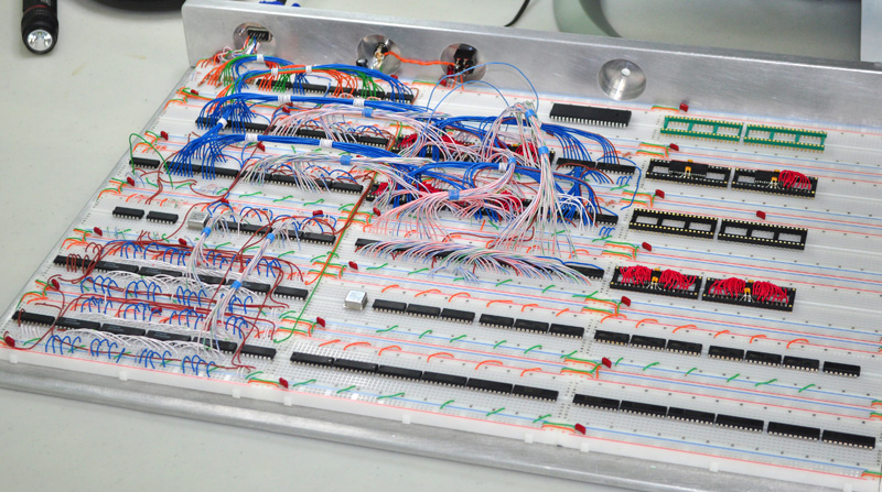
Planning a new silicon subdivision in Vulcan City.
The 43 new ICs outnumber the 40 ICs that make up the VGA Generator now.
The Sprite Generator is basically 2 large high speed X/Y counters that are "content aware".
Content aware meaning that alpha color and X/Y status are actually stored in the sprite data now.
Hopefully, this new design will translate well from paper to breadboard as it is a LOT to wire up!
Here is what each row of ICs currently do in the new design...
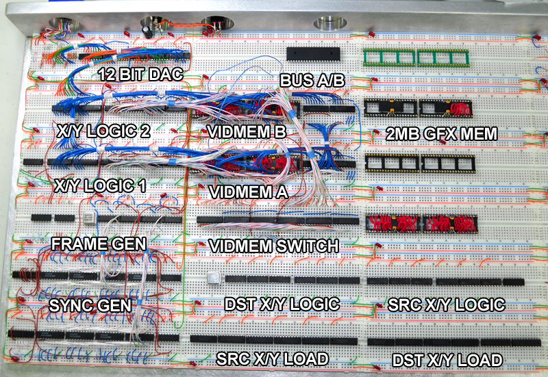
Each row of ICs have a specific job to do.
SRC and DST stand for Source and Destination.
Source Memory is the Sprite SRAM, and Destination is the VGA Memory (dual buffer).
You will notice that only 2 of my 8 SRAMs are presently wired to the sockets.
This is a time consuming job, and I have just finished cutting the other small 320 wires required.
In the old design, the Sprite Generator only had two 512K SRAMs, and now there are 8.
To get 16 bit SRAM, I have to double them up, and this time I also want twice the memory.
Expecting a massive speed increase, I am merging the PLayfield Generator into the Sprite Generator.
Image being able to scroll a huge 2048 x 1024 bitmap with 4096 colors around as a game background!
Even my current PC probably couldn't do it at 60FPS without missing a beat here and there!
Next time I have a day free, I intend to wire the Destination counters only, and run a block test.
I will see how fast I can push the new design when moving solid color blocks around the screen.
Until then... keep it retro dude!
Radical Brad
Here are the new chips that comprise the Sprite Generator...

Planning a new silicon subdivision in Vulcan City.
The 43 new ICs outnumber the 40 ICs that make up the VGA Generator now.
The Sprite Generator is basically 2 large high speed X/Y counters that are "content aware".
Content aware meaning that alpha color and X/Y status are actually stored in the sprite data now.
Hopefully, this new design will translate well from paper to breadboard as it is a LOT to wire up!
Here is what each row of ICs currently do in the new design...

Each row of ICs have a specific job to do.
SRC and DST stand for Source and Destination.
Source Memory is the Sprite SRAM, and Destination is the VGA Memory (dual buffer).
You will notice that only 2 of my 8 SRAMs are presently wired to the sockets.
This is a time consuming job, and I have just finished cutting the other small 320 wires required.
In the old design, the Sprite Generator only had two 512K SRAMs, and now there are 8.
To get 16 bit SRAM, I have to double them up, and this time I also want twice the memory.
Expecting a massive speed increase, I am merging the PLayfield Generator into the Sprite Generator.
Image being able to scroll a huge 2048 x 1024 bitmap with 4096 colors around as a game background!
Even my current PC probably couldn't do it at 60FPS without missing a beat here and there!
Next time I have a day free, I intend to wire the Destination counters only, and run a block test.
I will see how fast I can push the new design when moving solid color blocks around the screen.
Until then... keep it retro dude!
Radical Brad
- Oneironaut
- Posts: 734
- Joined: 25 May 2015
- Location: Gillies, Ontario, Canada
- Contact:
Re: Vulcan-74 - A 6502 Compatible Retro MegaProject
I am now wiring up an AVR to do some low level testing of the Source and Destination X/Y Counters.
This way, I can be sure of the results before going overboard on IO decoding to support the 6502.
Instead of asynchronous 74HC191 counters as in the previous design, I am now using synchronous 74HC163 counters.
The reason for this is due to the "look ahead" ability of the Load function, which will improve speed.
The downside is that these counters are absolute monsters to control.
Having to do everything on the clock transition is a serious pain, and adds a lot of extra circuitry.
But like I said... I would add 100 more ICs just to gain a single nanosecond!
When I have the initial test code ready, I will post a video of some boring moving mono color blocks.
These tests are so boring and time consuming to setup, but without a solid foundation, one can't build a house!
Later,
Brad
- Oneironaut
- Posts: 734
- Joined: 25 May 2015
- Location: Gillies, Ontario, Canada
- Contact:
Re: Vulcan-74 - A 6502 Compatible Retro MegaProject
Now that I am stuck indoors working on basement renos, I get the odd hour here and there to work on the Vulcan-74 board. It's nice to have a few breaks during the day, and have something to do while paint or drywall compound is drying!
As I mentioned, working with 74HC163 counters is so much more difficult than the 191 or 161 asynchronous variants.
Since you have to control the load line at the same time that the clock transitions, a lot of extra hardware is required.
How much more?... 20 ICs more, just to support the 2 sets of counters!
I am hoping for a few MHz of extra performance out of the Sprite Generator, so this is a huge deal.
If all of this fails to offer a speed increase, I will rip up the 163 counters and stomp on them all!
The second row of chips from the bottom make up the Source and Destination X/Y counters (12 74HC163s).
The row of 12 chips at the bottom are needed just to allow latching of the reset (Load) data into the counters...
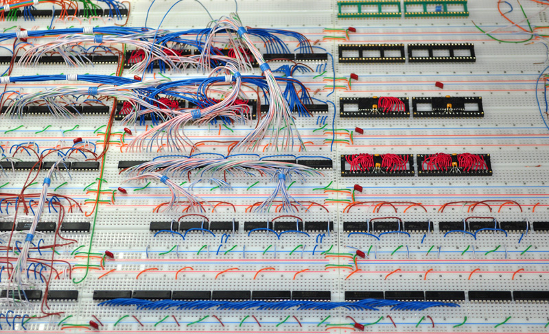
Adding the Counter Reset Registers.
Since the data to Load/Reset has to be present during a clock transition, it all has to be latched by the 6502 first.
The Blue wires represent the 8 bit Data Bus, and the white wires are address / counter outputs.
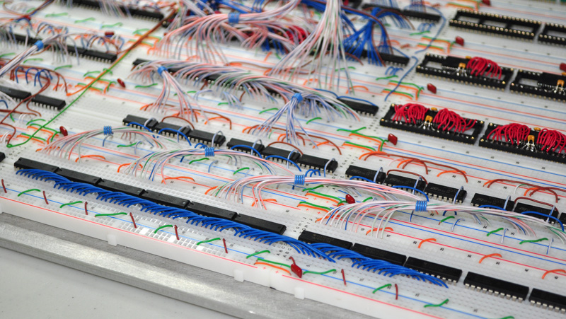
Destinations Counters connected to Video Memory.
The Address, Data, and WE lines are all fed into one last row of 74HC574 latches before hitting the SRAM.
I am still adding wires to do a basic test of the counters and latches.
Once I know what kind of speed to expect, I will add the automatic X/Y Wrap / Reset control logic.
I have a lot of code to write in order to run these tests.
Perhaps the next time I am painting, there will be time!
Cheers,
Radical Brad
As I mentioned, working with 74HC163 counters is so much more difficult than the 191 or 161 asynchronous variants.
Since you have to control the load line at the same time that the clock transitions, a lot of extra hardware is required.
How much more?... 20 ICs more, just to support the 2 sets of counters!
I am hoping for a few MHz of extra performance out of the Sprite Generator, so this is a huge deal.
If all of this fails to offer a speed increase, I will rip up the 163 counters and stomp on them all!
The second row of chips from the bottom make up the Source and Destination X/Y counters (12 74HC163s).
The row of 12 chips at the bottom are needed just to allow latching of the reset (Load) data into the counters...

Adding the Counter Reset Registers.
Since the data to Load/Reset has to be present during a clock transition, it all has to be latched by the 6502 first.
The Blue wires represent the 8 bit Data Bus, and the white wires are address / counter outputs.

Destinations Counters connected to Video Memory.
The Address, Data, and WE lines are all fed into one last row of 74HC574 latches before hitting the SRAM.
I am still adding wires to do a basic test of the counters and latches.
Once I know what kind of speed to expect, I will add the automatic X/Y Wrap / Reset control logic.
I have a lot of code to write in order to run these tests.
Perhaps the next time I am painting, there will be time!
Cheers,
Radical Brad
- Oneironaut
- Posts: 734
- Joined: 25 May 2015
- Location: Gillies, Ontario, Canada
- Contact:
Re: Vulcan-74 - A 6502 Compatible Retro MegaProject
Usually, I have all week to consider what to do next on the project if the weekend offers some free time.
I have been thinking about how to test the intricate timing / control for the X/Y counters using the AVR.
After some thought, I have decided to not do any testing, and instead wire up the entire Sprite Generator!
In reality, it does not matter if the AVR can swing the 32 control lines properly in code.
What matters is that everything works exactly as planned in real hardware at breakneck speed.
So I will be adding the Source Counters as well as the Graphics Memory and all of the support circuitry.
Wiring will be about 2 full days of work, or just one looooooong day's worth.
After the ten million wires are connected, I will have the AVR pretend to be a 6502, and try drawing a Sprite.
If the works, then I will move directly to the 6502 decode circuitry, and put my 65C02 back on the board.
until then....
Brad
- BigDumbDinosaur
- Posts: 9428
- Joined: 28 May 2009
- Location: Midwestern USA (JB Pritzker’s dystopia)
- Contact:
Re: Vulcan-74 - A 6502 Compatible Retro MegaProject
Oneironaut wrote:
Wiring will be about 2 full days of work, or just one looooooong day's worth.
After the ten million wires are connected, I will have the AVR pretend to be a 6502, and try drawing a Sprite.
If the works, then I will move directly to the 6502 decode circuitry, and put my 65C02 back on the board.
until then....
Brad
After the ten million wires are connected, I will have the AVR pretend to be a 6502, and try drawing a Sprite.
If the works, then I will move directly to the 6502 decode circuitry, and put my 65C02 back on the board.
until then....
Brad
x86? We ain't got no x86. We don't NEED no stinking x86!
- Oneironaut
- Posts: 734
- Joined: 25 May 2015
- Location: Gillies, Ontario, Canada
- Contact:
Re: Vulcan-74 - A 6502 Compatible Retro MegaProject
I am not sure I want to make a true PCB for it.
For sure, it will be taken from the breadboard and made into a real project, but most likely I will hand wire a board... point to point!
Even if I do eventually to a PCB, I will still take it through a hand wired board first.
The hand made oak / glass cabinet will have windows to both sides of the board to show off the insanity as well.
Brad
Quote:
Will this beast ever end up on a printed circuit board?
Last edited by Oneironaut on Wed Dec 14, 2016 9:18 pm, edited 1 time in total.
- BigDumbDinosaur
- Posts: 9428
- Joined: 28 May 2009
- Location: Midwestern USA (JB Pritzker’s dystopia)
- Contact:
Re: Vulcan-74 - A 6502 Compatible Retro MegaProject
Oneironaut wrote:
Even if I do eventually to a PCB, I will still take it through a hand wired board first.
The hand made oak / glass cabinet will have windows to both sides of the board to show off the insanity as well.
The hand made oak / glass cabinet will have windows to both sides of the board to show off the insanity as well.
x86? We ain't got no x86. We don't NEED no stinking x86!