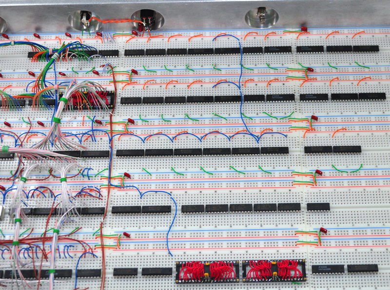
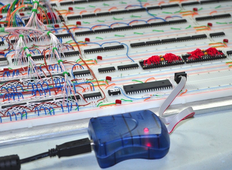
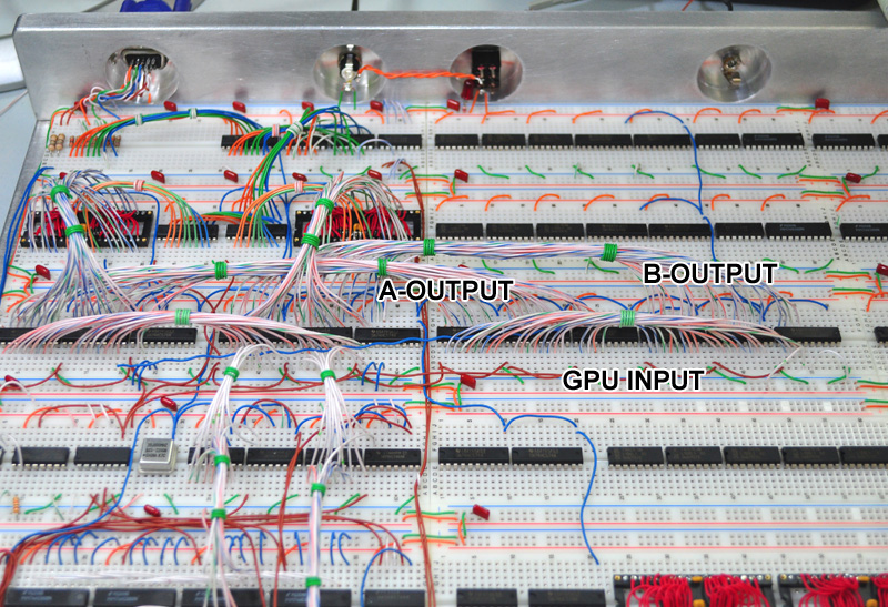
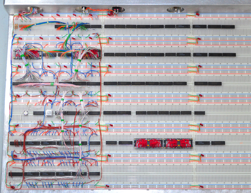
I did layout the GPU based on the messy diagram above, and might have enough time to test the XY counters tonight when the skeeters come out.
If my plan works, then this will be the GPU.
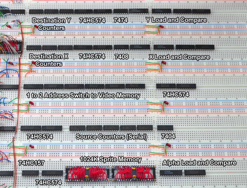
Who's who in the Solderless Zoo.
From the description above, this is how the GPU (should) work...
A 10 nanosecond bank of 1024K of memory (Graphics Memory) runs on its own isolated 20 bit address bus, fired by a series of 163 counters clocked at 20Mhz.
This is contiguous memory holding the "sprite data". The CPU can preset set the 163s with 20 bits of "Source Address".
The GMEM is clocked through 3 stages, with a series of 574s that keep propagation below 40ns, and allow switching to the dual buffer Video Memory.
As pixel data is pumped out of the GMEM, it is qualified with a known value set in the 688 comparator by the CPU, which is called "Alpha Color".
Any data NOT equaling Alpha, is sent to the VMEM data port, registered in sequence with the address and WE, controlled by the Alpha logic.
Data equaling the Alpha Value is considered "transparent", and is not drawn. This is how the GPU handles automatic transparent pixels at 20MHz.
On the "Destination" side of the logic, we have a split set of chained 163 counters running the X and Y address counters to the VMEM back buffer.
The CPU presets these values; Destination-X1 and X2, Destination Y1 and Y2. This tells the GPU where on the screen to draw the sprite block.
As you can see, sprites are not limited in any way, and can be as small as a single pixel, or as large as 512x512 due to the 9 bit XY addressing.
A few 688s control the resetting and wrapping of XY counters, and then trigger a "Ready" signal at the end of a sprite transfer.
This next stage in design will be more interesting for me since everything from here is untested.
Having done VGA designs in the past, the video section was not much of a challenge.
No doubt, there will be revisions, so wiring will be messy as I prototype the GPU!
Will try to make a few more posts this weekend.
Cheers,
Radical Brad