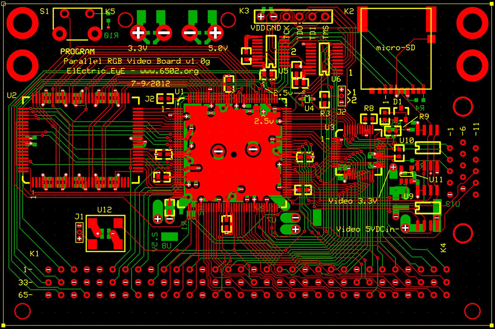
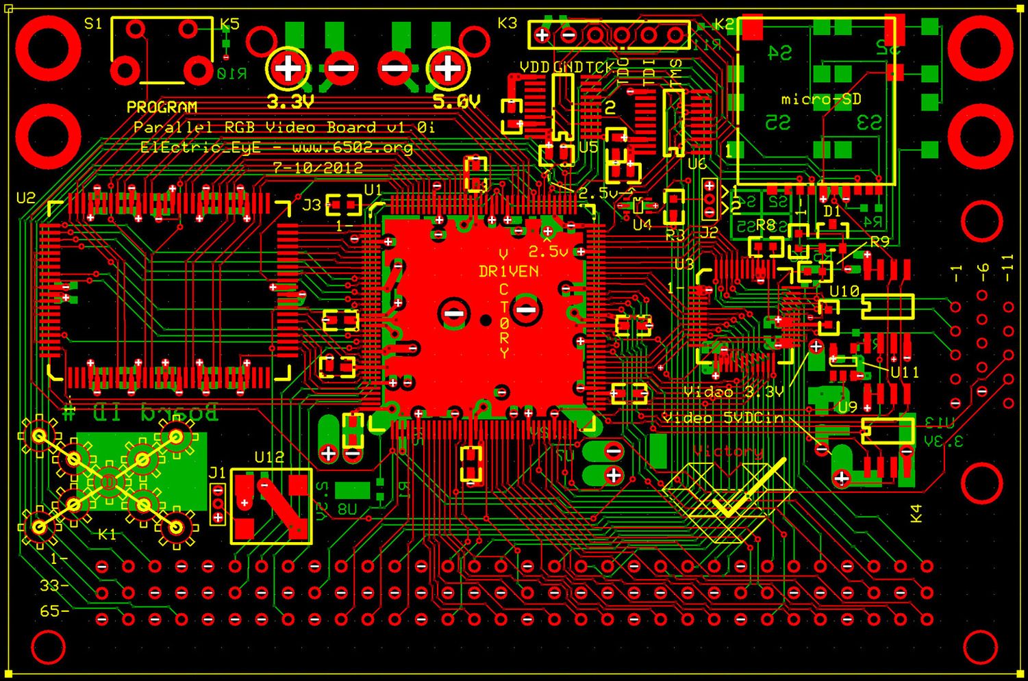
..Luckily, most of the important stuff is documented by the UCF file.
Yes, the .UCF file is key, also the parts list. I've taken pains to keep everything updated. Schematics are a pain nowadays and would slow my progress.
Some tips, in no particular order (parts are highlighted in white):
In regards to the:
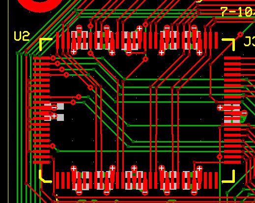
(U2) SyncRAM: 2 0603 bypass cap's fit on each power pin on the bottom of the board.
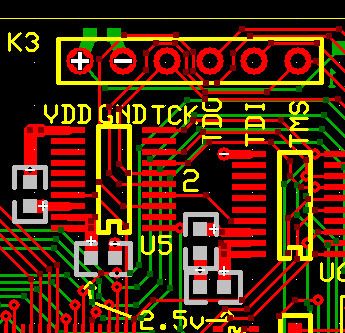
(U5 & U6) FPGA PROMs: 4 0603 bypass cap's on the top.
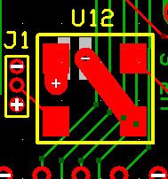
(U12) 100MHz Oscillator: 2 0603 cap's on the bottom.
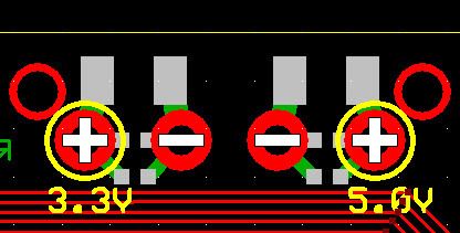
(3.3V & 5.0V mains): 2 1210 cap's, 4 0603 cap's on the bottom.
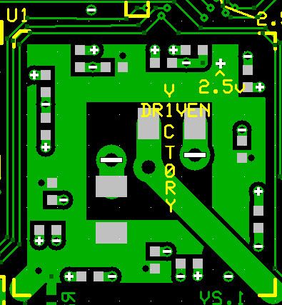
(U1): 7 0603 bypass cap's on top.
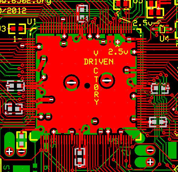
(U1): 14 0603 bypass cap's on bottom. 2 1210 bypass cap's on bottom center.
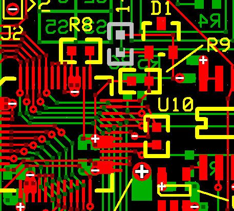
(U3): 1 0603 .1uF
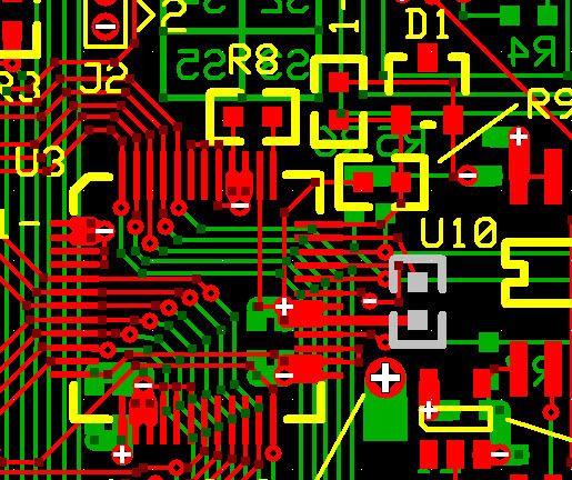
(U3): 1 0603 1uF
Now in retro, would've been easier for schematics, sorry.

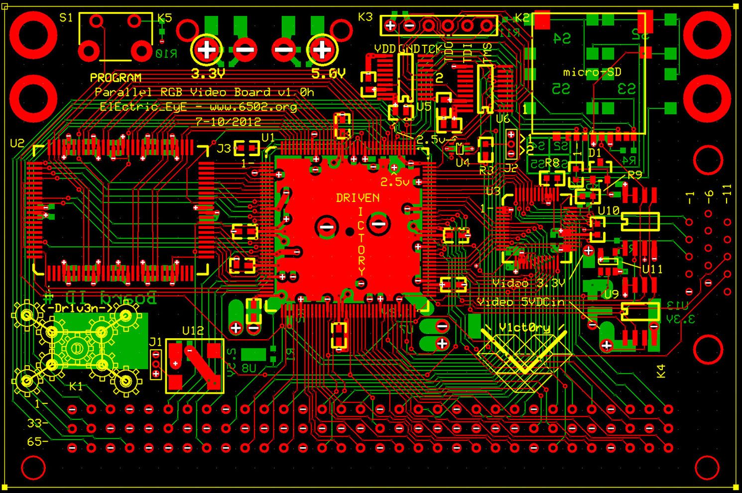
Pics are from v.0i, but everything is the same here. My mistake.

