PCB fabrication - manual drilling to stretch the hole budget

For discussing the 65xx hardware itself or electronics projects.
User avatar
Dr Jefyll
Posts: 3526
Joined: 11 Dec 2009
Location: Ontario, Canada
Contact:

PCB fabrication - manual drilling to stretch the hole budget

Post by Dr Jefyll »

Some of us have used the services of PCB houses that offer low-volume packages suitable for prototyping. For example I've had good results from ExpressPCB, and I'm sure there are other good suppliers out there. But sometimes the package deal comes with a limit on the number of holes, and that can constrain your design.
ManualDrilling7315.jpg
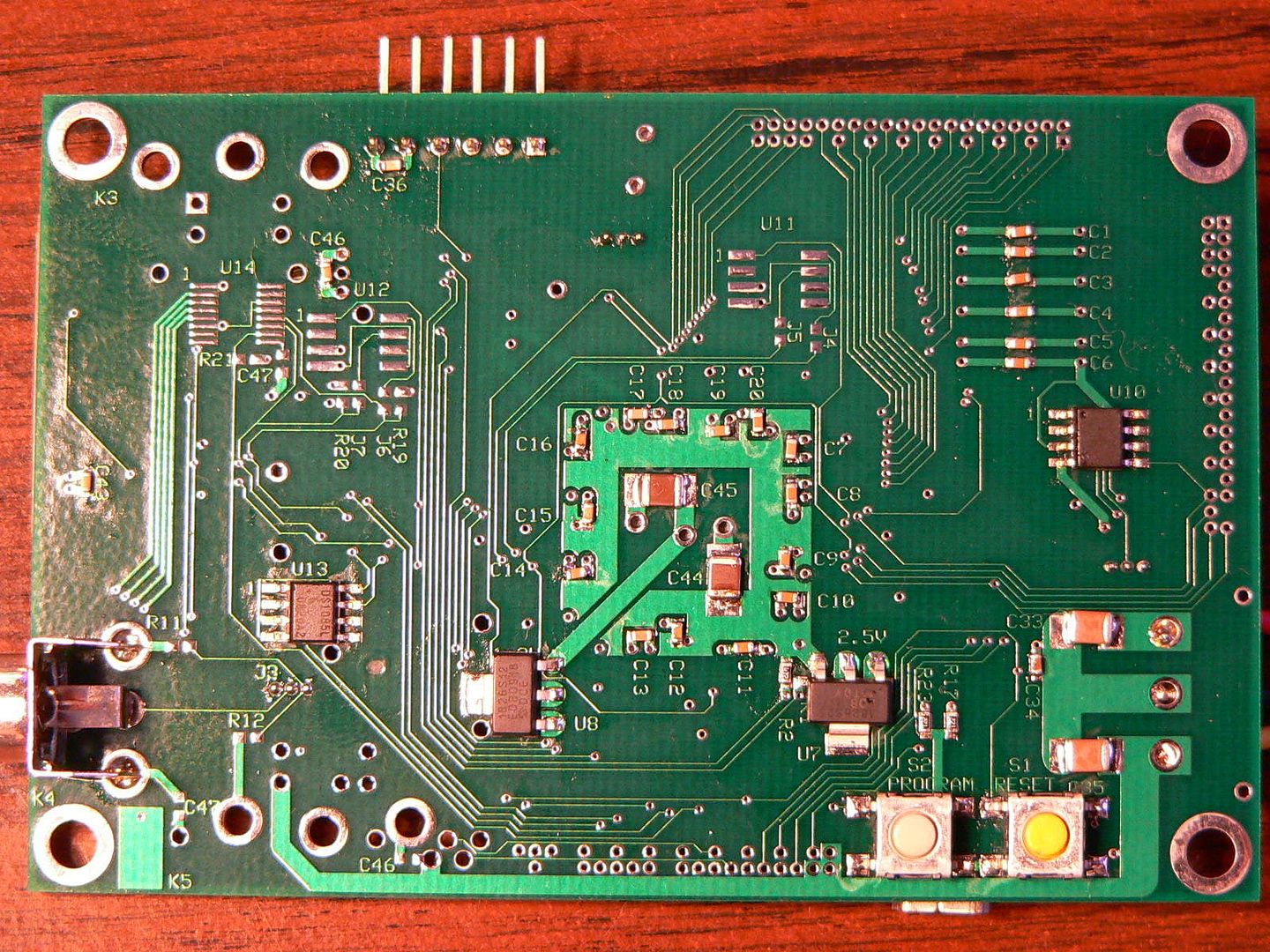
In case anyone finds the technique useful, here's a photo showing a project on which I was able to stretch the hole budget by manually drilling. In this case it allowed me to include some PLCC sockets which otherwise would have been been unaffordable, hole-wise.

The easiest way to add holes is with a hand-held electric drill. (Sometimes as a drilling template I use a scrap of pre-drilled proto-board material.) Hand-held drilling is adequate only for very simple cases.

The board in the photo was drilled on a vertical milling machine, with handwheels used to control X-Y position of the table. That worked out very conveniently, since one revolution of a handwheel would result in .1" of travel. :D Even so, it was imperative to use a center punch first, or else the tiny drill would "walk" off the slightly convex solder pads. IOW I had to begin by using X-Y positioning to center-punch every location to be drilled. After the dimples from the punch were precisely located, I found it was easy to do the actual drilling simply by hand-locating the PCB under the drill bit; the bit is flexible enough find the dimple despite any minor misalignment.

Obviously manual drilling is for low-volume and prototypes only. And of course there's no plate-through when you drill the hole yourself.

Jeff
http://LaughtonElectronics.com
Last edited by Dr Jefyll on Sat Apr 13, 2013 3:40 pm, edited 1 time in total.
User avatar
GARTHWILSON
Forum Moderator
Posts: 8775
Joined: 30 Aug 2002
Location: Southern California
Contact:

Post by GARTHWILSON »

You won't have the plate-thru though; so for IC sockects that cover the hole on the component side making it impossible to solder on that side, you'd have to limit the hand-drilling to pins whose connections are all on the bottom. (Good luck making CAD components for that, leaving out select holes.) One alternative I've thought of, but I don't know if it would be practical at all, is to put a fine strand of wire through the hole first and solder it on the top without blocking the hole, then putting the socket down, then soldering the pin to the bottom pad along with the fine strand of wire that already goes through the hole.

Vias are no problem, and I've even done repairs on a large Amek recording studio console (which may have been as much as $100,000 new) which had dozens of large, double sided PC boards without plated-thru holes, made around 1980 IIRC. This kind of thing is obviously not a high-volume production item, and the vias were just short wires that were soldered to both sides of the board, by hand.

In the case of multilayer boards, you're out of luck for connecting to inside layers. But to go to that much work, performance issues notwithstanding, one could just put jumper wires on the outside to substitute for the connections that could not be routed on a board of only two layers. Since such a board probably would not have a ground plane anyway, the jumper wires won't really degrade performance any further.
User avatar
PaulF
Posts: 143
Joined: 08 Dec 2008
Location: Brighton, England

Post by PaulF »

GARTHWILSON wrote:
One alternative I've thought of, but I don't know if it would be practical at all, is to put a fine strand of wire through the hole first and solder it on the top without blocking the hole, then putting the socket down, then soldering the pin to the bottom pad along with the fine strand of wire that already goes through the hole.
This is certainally possible, I did it myself years ago on a home-etched board. However, it is VERY fiddly and time consuming. It is usually easier to make a via somewhere else on the board - even if you have to drill the hole yourself and poke a wire through it and solder both sides.
Shift to the left,
Shift to the right,
Mask in, Mask Out,
BYTE! BYTE! BYTE!
User avatar
Dr Jefyll
Posts: 3526
Joined: 11 Dec 2009
Location: Ontario, Canada
Contact:

Post by Dr Jefyll »

PaulF wrote:
it is VERY fiddly and time consuming. It is usually easier to make a via somewhere else
Using a fine strand of wire to simulate a plate-through does sound like a fiddly job. I think occasions to use that trick would be rare, but to some extent the same can be said for my suggestion about manual drilling. IOW it's not what you'd choose for Standard Operating Procedure, but in certain circumstances the idea may prove expedient.

BTW the board in the photo is 2-layer; sorry for any confusion. Because of the risk of a short, I wouldn't suggest drilling a 4-layer board unless you can ensure the holes pass through a suitable void in the power planes. ExpressPCB's CAD software isn't highly sophisticated but it does allow you to specify "keep out" areas in the power planes. By including such areas I guess you could safely drill a 4-layer board after all.
GARTHWILSON wrote:
one could just put jumper wires on the outside [...] the jumper wires won't really degrade performance any further.
Right. For this particular project jumper wires are taken for granted as part of the plan.

-- Jeff
User avatar
Arlet
Posts: 2353
Joined: 16 Nov 2010
Location: Gouda, The Netherlands
Contact:

Post by Arlet »

People in Europe may be interested in http://www.eurocircuits.com/ for PCB manufacturing. Their proto service is reasonably priced, and has no limit on amount of holes drilled.
User avatar
8BIT
Posts: 1787
Joined: 30 Aug 2002
Location: Sacramento, CA
Contact:

Post by 8BIT »

Dr Jefyll wrote:
ExpressPCB's CAD software isn't highly sophisticated but it does allow you to specify "keep out" areas in the power planes. By including such areas I guess you could safely drill a 4-layer board after all.
In my experience with ExpressPCB, the "keep out" areas are used on the top or bottom layers only. I don't think they work on the inner power planes. I will test this this evening and if I find otherwise, I'll let you know.

Daryl
ElEctric_EyE
Posts: 3260
Joined: 02 Mar 2009
Location: OH, USA

Post by ElEctric_EyE »

8BIT wrote:
In my experience with ExpressPCB, the "keep out" areas are used on the top or bottom layers only. I don't think they work on the inner power planes. I will test this this evening and if I find otherwise, I'll let you know.

Daryl
The keep out areas work on the inner layers as well. In my project, the 2 inner layers are ground and 3.3VDC. There is an 'island' of 2.5V within the 3.3V layer.

You can see it if you look closely above C16, sort of an egg shape at an angle, it's a lighter shade of green.
User avatar
GARTHWILSON
Forum Moderator
Posts: 8775
Joined: 30 Aug 2002
Location: Southern California
Contact:

Post by GARTHWILSON »

Quote:
Because of the risk of a short, I wouldn't suggest drilling a 4-layer board unless you can ensure the holes pass through a suitable void in the power planes. ExpressPCB's CAD software isn't highly sophisticated but it does allow you to specify "keep out" areas in the power planes. By including such areas I guess you could safely drill a 4-layer board after all.
The RS-274X gerber standard is not difficult to understand, and if you need to make some little mod that your CAD won't do, you can go into the resulting gerber files and edit them with a common text editor. I do it frequently. Removing an inner-layer pad around a hole would be a very quick job. To make sure I didn't goof, I check the result in Gerbv, a free gerber viewer for Linux, before zipping the files and sending them to the board house. Edit, 12/1/16: I see there's a free 3D online gerber viewer at http://mayhewlabs.com/3dpcb .
http://WilsonMinesCo.com/ lots of 6502 resources
The "second front page" is http://wilsonminesco.com/links.html .
What's an additional VIA among friends, anyhow?
User avatar
8BIT
Posts: 1787
Joined: 30 Aug 2002
Location: Sacramento, CA
Contact:

Post by 8BIT »

ElEctric_EyE wrote:
8BIT wrote:
In my experience with ExpressPCB, the "keep out" areas are used on the top or bottom layers only. I don't think they work on the inner power planes. I will test this this evening and if I find otherwise, I'll let you know.

Daryl
The keep out areas work on the inner layers as well. In my project, the 2 inner layers are ground and 3.3VDC. There is an 'island' of 2.5V within the 3.3V layer.

You can see it if you look closely above C16, sort of an egg shape at an angle, it's a lighter shade of green.
Well I'll be darned - I was wrong. I guess I never tried it. I give EPCB credit, they are always adding to their software.

My apologies for the misinformation!

Daryl
User avatar
davejo
Posts: 1
Joined: 03 Aug 2012

Re:

Post by davejo »

GARTHWILSON wrote:
Quote:
Because of the risk of a short, I wouldn't suggest drilling a 4-layer board unless you can ensure the holes pass through a suitable void in the power planes. ExpressPCB's CAD software isn't highly sophisticated but it does allow you to specify "keep out" areas in the power planes. By including such areas I guess you could safely drill a 4-layer board after all.
The RS-274X gerber standard is not difficult to understand, and if you need to make some little mod that your CAD won't do, you can go into the resulting gerber files and edit them with a common text editor. I do it frequently. Removing an inner-layer pad around a hole would be a very quick job. To make sure I didn't goof, I check the result in Gerbv, a free gerber viewer for Linux, before zipping the files and sending them to the board house.
can you provide me with a link to free gerber viewer for linux? i need it very urgently for one of my projects.

thanks in advance

dave
User avatar
GARTHWILSON
Forum Moderator
Posts: 8775
Joined: 30 Aug 2002
Location: Southern California
Contact:

Re: PCB fabrication - manual drilling to stretch the hole bu

Post by GARTHWILSON »

Welcome Dave. I got it from the Ubuntu Software Center. If you have Ubuntu, type "gerbv" in the software center search and it will come right up, and a single click downloads and installs it. If your Linux is something else, you might need to go to http://gerbv.gpleda.org/ which came up when I went into the "Help" in Gerbv. It looks like everything you need is there. Edit, 12/1/16: I see there's a free 3D online gerber viewer at http://mayhewlabs.com/3dpcb .
http://WilsonMinesCo.com/ lots of 6502 resources
The "second front page" is http://wilsonminesco.com/links.html .
What's an additional VIA among friends, anyhow?
User avatar
BigEd
Posts: 11464
Joined: 11 Dec 2008
Location: England
Contact:

Re: PCB fabrication - manual drilling to stretch the hole bu

Post by BigEd »

Just for interest: Andrew Huang's piece about a PCB factory in Italy
http://www.bunniestudios.com/blog/?p=2407
User avatar
Dajgoro
Posts: 808
Joined: 08 Aug 2011
Location: Croatia
Contact:

Re: PCB fabrication - manual drilling to stretch the hole bu

Post by Dajgoro »

I didn't know that there was a mini silicon valley in Italy, its kinda close to where i live...
User avatar
BigDumbDinosaur
Posts: 9428
Joined: 28 May 2009
Location: Midwestern USA (JB Pritzker’s dystopia)
Contact:

Re: PCB fabrication - manual drilling to stretch the hole bu

Post by BigDumbDinosaur »

Dajgoro wrote:
I didn't know that there was a mini silicon valley in Italy, its kinda close to where i live...

It's right next door to one of the best Italian restaurants in the known solar system. :lol: Actually I don't know if that's true but a friend who was in Italy for the 2006 Winter Olympics said he ate like a king every night he was there and put on at least 10 pounds by the time he got ready to come home. He said the experience spoiled him for Italian restaurants in the USA.
x86?  We ain't got no x86.  We don't NEED no stinking x86!
User avatar
Dajgoro
Posts: 808
Joined: 08 Aug 2011
Location: Croatia
Contact:

Re: PCB fabrication - manual drilling to stretch the hole bu

Post by Dajgoro »

My kind of food... I love spaghetti bolognese and other stuff...
The food over here is not much different, and if you find the right place, you can spend all of your money :mrgreen: . The only issue is that i am living in a perfect vacation spot full of tourists from Italy, Germany, UK... but no IT/electronics industry whatsoever.
I know there was some industry going in Italy in before, i even have a old hard drive that was made there. Before the war we had some electronic industry too, but now everything is going to hell over here, so i guess if i am going to order pcb boards i am going to drill every hole myself...
Post Reply