That's some good info!
I'm still having trouble. But I have narrowed it down some. Let me explain.
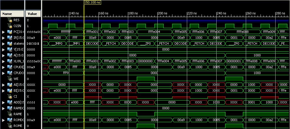
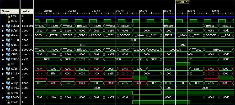
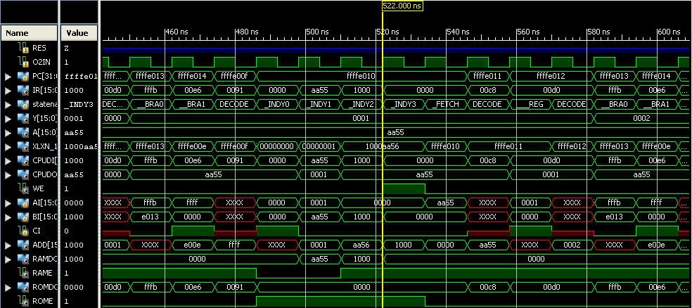
First, I started to focus at the very beginning of the simulation where trouble is first starting with the indirect indexed mode. Using the same program I mentioned before, it is supposed to store $AA55 from $10000000 to $FFFEFFFF using a STA($0000),y.
In the first store it successfully writes to $10000000. The very next store it erroneously writes to $1000AA56. Which means $AA55 is being written to $00000000 at some point before this.
Looking at ISim (even in extreme magnification), there is no instance when there is a high WE, a low to select RAM, and an address $00000000.
This leads me to believe 1 of 3 things are happening: Either I am failing to initialize an internal register to properly see a simulation, the core is acting strangely after the 16-bit modifications, or I am losing my mind.
The last is quite possible!
My branch offsets are correct aren't they?
65ORG16.b Core
-
ElEctric_EyE
- Posts: 3260
- Joined: 02 Mar 2009
- Location: OH, USA

-
ElEctric_EyE
- Posts: 3260
- Joined: 02 Mar 2009
- Location: OH, USA

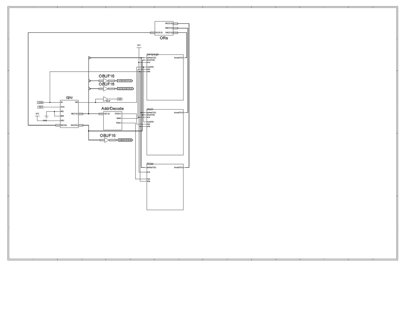
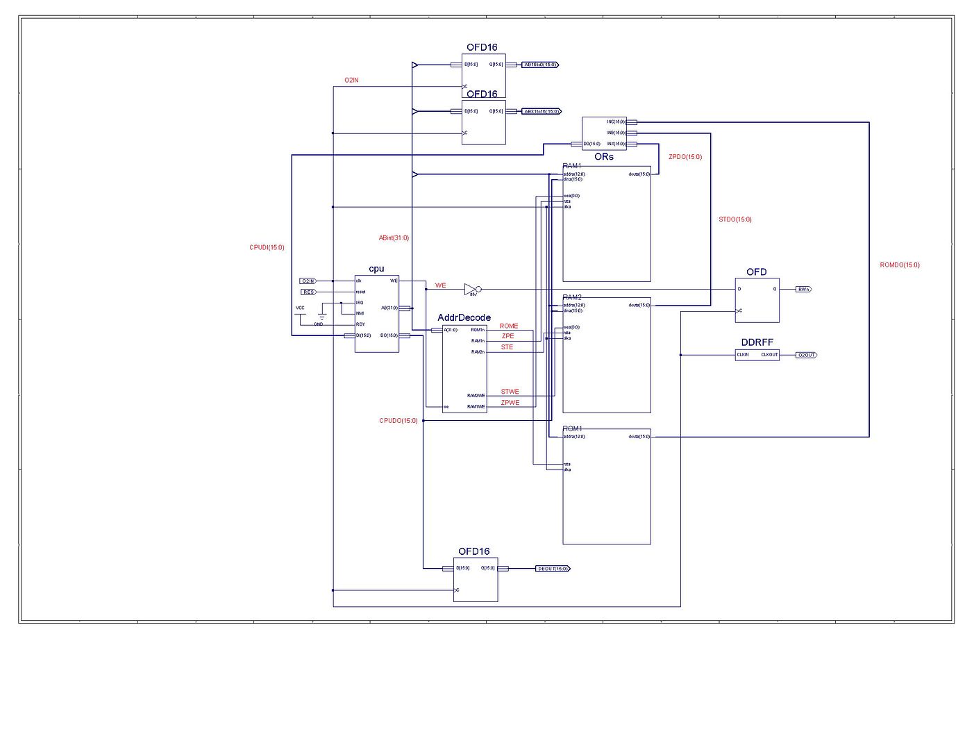
You've posted some schematics earlier. Are those still valid ?
top level schematics
It looks like you have WE hooked up directly to the block RAM WE input. The RAM enable input is tied to Vcc. If that's the case, any write will overwrite something in the block RAM. The fact that you assert the SSR (reset) input of the RAM at the same time, doesn't prevent this. According to XAPP463, page 20:
You'll need to mix in the address decoding in the enable signal as well. This is how I did it (EN_RAM0 is the enable signal, and is used for both the SSR input and the the WE input).
top level schematics
It looks like you have WE hooked up directly to the block RAM WE input. The RAM enable input is tied to Vcc. If that's the case, any write will overwrite something in the block RAM. The fact that you assert the SSR (reset) input of the RAM at the same time, doesn't prevent this. According to XAPP463, page 20:
Quote:
Simultaneous Write and Synchronous Set/Reset Operations
If a simultaneous write operation occurs during the synchronous set/reset operation, then the data on the DI and DIP inputs is stored at the RAM location specified by the ADDR input. However, the data output latches are initialized to the SRVAL attribute value as described immediately above.
If a simultaneous write operation occurs during the synchronous set/reset operation, then the data on the DI and DIP inputs is stored at the RAM location specified by the ADDR input. However, the data output latches are initialized to the SRVAL attribute value as described immediately above.
Code: Select all
        .CLKA( clk ),
        .WEA( WE & EN_RAM0 ),
        .ENA( 1'b1 ),
        .SSRA( ~EN_RAM0 ),
        .ADDRA( AB[10:0] ),
        .DOA( DO_RAM0 ),
        .DIA( DI ),
-
ElEctric_EyE
- Posts: 3260
- Joined: 02 Mar 2009
- Location: OH, USA
Yes, those schematics are up to date...
Thank you so much, my friend!
I'll read up on the equivalent Spartan 6 BRAM User Guide and make the necessary changes. I'm sure they're functionally identical...
I can't believe I got away with this technique for so long. I guess in the 6502SoC, with a register based display and a small window into a large Flash, this problem did not reveal itself.
Hi EE
I ran your program in my setup: I seemed to have the same problem. In my case it was because of the small RAM being aliased, so writes to $1000_0000 were in fact overwriting the pointer at $0000_0000 - to avoid that hazard, it's safer perhaps to initialise the destination pointer to $1000_0002
Once I'd done that, it worked as expected.
Cheers
Ed
-
ElEctric_EyE
- Posts: 3260
- Joined: 02 Mar 2009
- Location: OH, USA
Arlet wrote:
...It looks like you have WE hooked up directly to the block RAM WE input... If that's the case, any write will overwrite something in the block RAM. The fact that you assert the SSR (reset) input of the RAM at the same time, doesn't prevent this. According to XAPP463, page 20:
You'll need to mix in the address decoding in the enable signal as well. This is how I did it (EN_RAM0 is the enable signal, and is used for both the SSR input and the the WE input).
Quote:
Simultaneous Write and Synchronous Set/Reset Operations
If a simultaneous write operation occurs during the synchronous set/reset operation, then the data on the DI and DIP inputs is stored at the RAM location specified by the ADDR input. However, the data output latches are initialized to the SRVAL attribute value as described immediately above.
If a simultaneous write operation occurs during the synchronous set/reset operation, then the data on the DI and DIP inputs is stored at the RAM location specified by the ADDR input. However, the data output latches are initialized to the SRVAL attribute value as described immediately above.
Code: Select all
        .CLKA( clk ),
        .WEA( WE & EN_RAM0 ),
        .ENA( 1'b1 ),
        .SSRA( ~EN_RAM0 ),
        .ADDRA( AB[10:0] ),
        .DOA( DO_RAM0 ),
        .DIA( DI ),
Best out of 7, using SmartXplorer, got it to 86.7MHz with a xc6slx9 tqg144 -3. They were all within a couple MHz difference though, with a 12ns O2IN constraint. The .b core has no BCD mode, i.e. no SED ($00F8) & CLD ($00C8) opcodes, but does have all other original 6502 ($00xx) opcodes.
-
ElEctric_EyE
- Posts: 3260
- Joined: 02 Mar 2009
- Location: OH, USA
I am one step away from implementing 3 more 16-bit Accumulator's, as I followed Arlet's advice quoted in my very first post in this thread...
If they work, the next plan is to implement a 16x16 bit multiplier using A and B accumulators, then putting the MSB result in the C accumulator and LSB in the D accumulator, while keeping the X and Y index registers.
If they work, the next plan is to implement a 16x16 bit multiplier using A and B accumulators, then putting the MSB result in the C accumulator and LSB in the D accumulator, while keeping the X and Y index registers.
ElEctric_EyE wrote:
If they work, the next plan is to implement a 16x16 bit multiplier using A and B accumulators, then putting the MSB result in the C accumulator and LSB in the D accumulator, while keeping the X and Y index registers.
-
ElEctric_EyE
- Posts: 3260
- Joined: 02 Mar 2009
- Location: OH, USA
I'm updating the top level schematics of the "testbench" to include output FF's. I'm starting from scratch since I'm using ISE13.2. I think I was using 12.4 back then (in June).
Then I'll try to write a simple load and store from the B accumulator using macros to define the new opcodes and see what it looks like in ISim.
I'm not 100% following you with the cycles, but I do see I need to include the new opcode values in the state machine. Give me just a few hours to get the testbench sorted out, and also to re-check over the cpu.V file and I will try to post what I have modified, regarding the core, on github.
Then I'll try to write a simple load and store from the B accumulator using macros to define the new opcodes and see what it looks like in ISim.
Arlet wrote:
...Keep in mind you'll need two cycles to store the results, since the register file can only access a single register at a time. You'll need to create an extra state in the opcode state machine.
-
ElEctric_EyE
- Posts: 3260
- Joined: 02 Mar 2009
- Location: OH, USA
Arlet, I've fully updated the 65Org16.b core with most of your own modifications from your latest posting on Github for your 6502 core.
I believe there is a problem? with the modifications you made to lines 982 & 984. I'm testing the 65Org16.b core in the Devboard and it all works fine until I make the mod at the bottom.
BEFORE(working)
AFTER(not working)
I believe there is a problem? with the modifications you made to lines 982 & 984. I'm testing the 65Org16.b core in the Devboard and it all works fine until I make the mod at the bottom.
BEFORE(working)
Code: Select all
982     8'bxxxx_10x0,	     // ASLA, ROLA, LSRA, RORA, Txx, DEX, NOP,
983     8'bxxx0_1000,	     // PHP, PLP, PHA, PLA, DEY, TAY, INY, INX
984 ...Code: Select all
982     8'bxxxx_1010,	     // ASLA, ROLA, LSRA, RORA, T[XS][SX], DEX, NOP,
983     8'bxxx0_1000,	     // PHP, PLP, PHA, PLA, DEY, TAY, INY, INX
984 8'b1001_1000, // TYAElEctric_EyE wrote:
Arlet, I've fully updated the 65Org16.b core with most of your own modifications from your latest posting on Github for your 6502 core.
I believe there is a problem? with the modifications you made to lines 982 & 984. I'm testing the 65Org16.b core in the Devboard and it all works fine until I make the mod at the bottom.
BEFORE(working)
AFTER(not working)
I believe there is a problem? with the modifications you made to lines 982 & 984. I'm testing the 65Org16.b core in the Devboard and it all works fine until I make the mod at the bottom.
BEFORE(working)
Code: Select all
982     8'bxxxx_10x0,	     // ASLA, ROLA, LSRA, RORA, Txx, DEX, NOP,
983     8'bxxx0_1000,	     // PHP, PLP, PHA, PLA, DEY, TAY, INY, INX
984 ...Code: Select all
982     8'bxxxx_1010,	     // ASLA, ROLA, LSRA, RORA, T[XS][SX], DEX, NOP,
983     8'bxxx0_1000,	     // PHP, PLP, PHA, PLA, DEY, TAY, INY, INX
984 8'b1001_1000, // TYACan you narrow it down to a specific instruction in your simulations ?
-
ElEctric_EyE
- Posts: 3260
- Joined: 02 Mar 2009
- Location: OH, USA
I will try to find out... The Devboard is initializing the display properly, which is a bunch of LDA/STA and LDX,DEX, BNE (for small delay to init TFT PLL)...
I've just finished my testbench which is good incidental timing. Top level signals are in red for when I post future sims, which in this case won't really matter since we'll be looking at internal CPU signals. For simplicity's sake in this testbench, the ZeroPage/Stack/ROM blockRAM's are 8Kx16 each fully address decoded. I'll post the innards any of the modules if needed.
I'll try to find out where the problem might be, write a simple program and follow it in ISim...
Aside from ISim, I am putting this core to use in real life on V1.1 of the Devboard as well, since a simulation won't reveal all.
-
ElEctric_EyE
- Posts: 3260
- Joined: 02 Mar 2009
- Location: OH, USA
Ok, I've found out the DEY instruction is not working on the devboard and confirmed by simulation on the testbench... I had rearranged the AXYS parameter assignments for 'd0 - 'd4. Maybe I shouldn't have done this? I'll try putting it back in 'order'.
This doesn't matter...
Woops, sorry, I had forgotten to add line 983 from your master thread to my 65Org16.b! (946 on 65Org16.b)
Now I have a viable core, time to add accumulators!
Updated cpu.v & ALU.v on Github. PITA.
At this point top speed is 100MHz.
Code: Select all
parameter
	SEL_A    = 2'd3,
	SEL_X	 = 2'd2,
	SEL_Y    = 2'd1,
SEL_S = 2'd0;Woops, sorry, I had forgotten to add line 983 from your master thread to my 65Org16.b! (946 on 65Org16.b)
Code: Select all
983 8'bxxx0_1000, // PHP, PLP, PHA, PLA, DEY, TAY, INY, INXUpdated cpu.v & ALU.v on Github. PITA.
At this point top speed is 100MHz.
Last edited by ElEctric_EyE on Thu Feb 23, 2012 12:09 am, edited 1 time in total.
-
ElEctric_EyE
- Posts: 3260
- Joined: 02 Mar 2009
- Location: OH, USA
No success yet. Just thought I'd share what I've got so far...
Opcodes for the B Accumulator are simple, not thought through at all.
For example, an LDA #$xxxx would look like $00A9, $xxxx in Hex Editor.
With a B Accumulator, a Macro/.BYTE on As65 using an LDB #$xxxx presently looks like $A9A9, $xxxx.
Following this thought process will not allow for further opcode expansion regarding Accumulators. I'm just concentrating on getting the first B Accumulator functional, then I can think on how to properly expand the opcode set further...
Since regsel has now been expanded to 3bits, there is the opportunity for 8 16-bit registers in the regfile.
Only 5 (B,A,X,Y,S) are being used now:
Code: Select all
reg [2:0] regsel;			// Select B, A, X, Y or S register
wire [15:0] regfile = BAXYS[regsel];	// Selected register output
Code: Select all
reg [15:0] BAXYS[4:0]; // B, A, X, Y and S register fileCode: Select all
parameter
	SEL_A	 = 3'd0,
	SEL_S    = 3'd1,
	SEL_X	 = 3'd2,
	SEL_Y    = 3'd3,
	SEL_B    = 3'd4;

initial
	begin
		BAXYS[SEL_B] = 0; //init 2nd accumulator
		BAXYS[SEL_A] = 0; //init accumulator
		BAXYS[SEL_X] = 0; //init x register
		BAXYS[SEL_Y] = 0; //init y register
		BAXYS[SEL_S] = 16'hffff; //init stack
	end
Code: Select all
reg [2:0] src_reg;	// source register index
reg [2:0] dst_reg;	// destination register index