6502.org Forum  Projects  Code  Documents  Tools  Forum
It is currently Sat Nov 23, 2024 1:29 am

All times are UTC


Post new topic Reply to topic  [ 224 posts ]  Go to page Previous  1 ... 11, 12, 13, 14, 15  Next
Author Message
 Post subject:
PostPosted: Tue Apr 19, 2011 9:15 pm 
Offline

Joined: Mon Mar 02, 2009 7:27 pm
Posts: 3258
Location: NC, USA
OK, cool. I see the declaration in the cpu module:
Code:
reg  [7:0] AXYS[3:0];    // A, X, Y and S register file


I would've responded earlier...

I got sidetracked setting up my old C-64 system and decided to start a new thread for the software side of 6502SoC.

Back to working on the 6502SoC Flash interface tomorrow...


Top
 Profile  
Reply with quote  
 Post subject:
PostPosted: Wed Apr 20, 2011 1:49 pm 
Offline

Joined: Mon Mar 02, 2009 7:27 pm
Posts: 3258
Location: NC, USA
OK, I think I got the Flash interface working @6MHz, finally! Using a top level bidirectional data bus is a very important building block. The display is clearing Black and reading $FF from the Flash and displaying White as expected...

Now plans are to use RDY.
ISE is saying Max Frequency of the project is @54.8MHz. I would like to run the CPU @48MHz now, put wait states to interface to the Display @38MHz, and more wait states to interface to the Flash @6MHz.


Top
 Profile  
Reply with quote  
 Post subject:
PostPosted: Wed Apr 20, 2011 2:43 pm 
Offline
User avatar

Joined: Tue Nov 16, 2010 8:00 am
Posts: 2353
Location: Gouda, The Netherlands
You could run the CPU at 48 MHz, and have a simple RDY signal that's '1' for one cycle, and '0' for 7 cycles. This should produce the same results as your 6 MHz test, and should be easy to set up.


Top
 Profile  
Reply with quote  
 Post subject:
PostPosted: Wed Apr 20, 2011 7:11 pm 
Offline

Joined: Mon Mar 02, 2009 7:27 pm
Posts: 3258
Location: NC, USA
Arlet wrote:
You could run the CPU at 48 MHz, and have a simple RDY signal that's '1' for one cycle, and '0' for 7 cycles. This should produce the same results as your 6 MHz test, and should be easy to set up.


Shoot, I did mean 12MHz for the Flash. Sorry, my brain needs a rest!
But the RDY is an easy 1:4 ratio from the Flash 12MHz to the CPU 48MHz, unlike the 4:5 ratio of the Video 38MHZ to CPU 48MHz.
I have to get the Flash and the Display working together for me to test.


Top
 Profile  
Reply with quote  
 Post subject:
PostPosted: Thu Apr 21, 2011 6:47 pm 
Offline

Joined: Mon Mar 02, 2009 7:27 pm
Posts: 3258
Location: NC, USA
OK I needed to get in the right frame of mind to think about this, aside from the excitement of firing up the 64 again. What better place than work to remove that excitement!...
This is what I understand so far:
From looking at Daryl's (8bit) and BDD's wait state circuits, I need to assert/deassert RDY during Phase 2 high.
RDY will be applied only during chip select actives.
The amount of time RDY is held active is the variable I need to find out for each device.
But to give me better resolution for the RDY active time, I think a good thing to do would be to use a DCM to double the phase 2 frequency to 97MHz (48.58x2)...


Top
 Profile  
Reply with quote  
 Post subject:
PostPosted: Thu Apr 21, 2011 7:01 pm 
Offline
User avatar

Joined: Tue Nov 16, 2010 8:00 am
Posts: 2353
Location: Gouda, The Netherlands
The 6502 core won't go as fast as 97MHz. I also don't have phase 1/phase 2 clocks in my core, just a single clock input.

The RDY signal needs to be asserted/deasserted on rising edges of this clock, just like any other input/output signal to the core.

Also, don't forget there's an extra cycle delay when the core reads from memory. It presents the address on the AB bus, and on the next cycle, it expects the data on DI.


Top
 Profile  
Reply with quote  
 Post subject:
PostPosted: Thu Apr 21, 2011 7:14 pm 
Offline

Joined: Mon Mar 02, 2009 7:27 pm
Posts: 3258
Location: NC, USA
Arlet wrote:
The 6502 core won't go as fast as 97MHz. I also don't have phase 1/phase 2 clocks in my core, just a single clock input...

The cpu would still run @48.58MHz... The 97MHz would run a 2 to 4 bit counter to feed RDY, and would count 0 to X(whatever is needed for each device) on the rising edge (both frequency's would have the same rising edge since 1 is just 2X the other). It would give finer resolution to avoid delaying the CPU any more than absolutely necessary.

Arlet wrote:
...The RDY signal needs to be asserted/deasserted on rising edges of this clock, just like any other input/output signal to the core.

Rising edges, yes. I need to think edges, not levels, especially since FF's are involved.

Arlet wrote:
...Also, don't forget there's an extra cycle delay when the core reads from memory. It presents the address on the AB bus, and on the next cycle, it expects the data on DI.

I have a FF for the Flash RE signal delaying it one cycle. The Flash WE is just logic, no FF.
Actually, the same is true for my 2 Flash bank address registers(A10-A17) and (A18-A20, 5 bits unused). I think I also have the Flash CS delayed one cycle too. I will have to check about the CS when I get home tonight, I have the newest project files on another computer at home. Forgot to update this computer...
__________________________________________________________________________________________________________________________
No, the CS is not delayed. I know this would've screwed up the WE, but at one point I was testing this scenario.

Top
 Profile  
Reply with quote  
 Post subject:
PostPosted: Fri Apr 22, 2011 5:12 am 
Offline
User avatar

Joined: Tue Nov 16, 2010 8:00 am
Posts: 2353
Location: Gouda, The Netherlands
ElEctric_EyE wrote:
Arlet wrote:
The 6502 core won't go as fast as 97MHz. I also don't have phase 1/phase 2 clocks in my core, just a single clock input...

The cpu would still run @48.58MHz... The 97MHz would run a 2 to 4 bit counter to feed RDY, and would count 0 to X(whatever is needed for each device) on the rising edge (both frequency's would have the same rising edge since 1 is just 2X the other). It would give finer resolution to avoid delaying the CPU any more than absolutely necessary.


There's no point in letting the RDY go faster than the CPU clock. You can only delay the CPU by whole clock cycles. Also, I would let the RDY delay counter count down, that way you only need to test for 0.

As far as the delay cycle, it's best to put flip-flops on the AB output, the DO, the WE, and the CS (CS needs to be derived from original AB). That way, all signals have nice clean edges at the same time, without any glitches, as they leave the FPGA. There are special flip-flops built into the pads for this purpose, and the tool is smart enough to use those.


Top
 Profile  
Reply with quote  
 Post subject:
PostPosted: Fri Apr 22, 2011 12:38 pm 
Offline

Joined: Mon Mar 02, 2009 7:27 pm
Posts: 3258
Location: NC, USA
Ok, understood about the RDY cycle. I'm making a new module for it and will be able to test it in the next few days.

Arlet wrote:
...As far as the delay cycle, it's best to put flip-flops on the AB output, the DO, the WE, and the CS...


I seem to have done an inverse, and delayed the RE only, and it seems to work.
But you are saying to delay ABout, DO, and WE and not RE?


Top
 Profile  
Reply with quote  
 Post subject:
PostPosted: Fri Apr 22, 2011 1:17 pm 
Offline
User avatar

Joined: Tue Nov 16, 2010 8:00 am
Posts: 2353
Location: Gouda, The Netherlands
I think it's best to delay all outputs, including RE. The idea is that everything will then be synchronous, but just 1 cycle delayed. The extra flip flops will create nice clean edges and the tools can guarantee you meet the timing requirements.

With a bunch of combinatorial signals, you never know which signal will come first. You don't want WE to be asserted when AB is still unstable.

ETA: Also, when you delay everything equally, you won't have a problem with alternating read/write cycles. For instance, when you only delay RE, and you do a read cycle, followed by a write, the original WE and the delayed RE will be asserted at the same time. Therefore you'll need to delay WE as well, and if you delay WE, you'll need to delay AB and DO, otherwise you write the wrong data in the wrong address.


Top
 Profile  
Reply with quote  
 Post subject:
PostPosted: Sat Apr 23, 2011 12:01 am 
Offline

Joined: Mon Mar 02, 2009 7:27 pm
Posts: 3258
Location: NC, USA
Ok, that does make sense, alot of sense!

I will have a chance to put this concept to work by the end of Sunday. Also, will try the RDY circuit, and report back.


Top
 Profile  
Reply with quote  
 Post subject:
PostPosted: Sun Apr 24, 2011 10:47 pm 
Offline

Joined: Mon Mar 02, 2009 7:27 pm
Posts: 3258
Location: NC, USA
The RDY concept is perplexing me, unable to post progress, because I don't full understand the concept. Gonna put it on the back burner for the moment and continue progressing on the software hack side...

But I did put all WE and RE signals through FF's successfully. Also the 6502 DOs, the ones that go offchip. The DOs for the internal bidirectional ports don't need to be delayed. Also, the ABInt does not need to be delayed. ISE gave a mention that they were already qualified by O2.


Top
 Profile  
Reply with quote  
 Post subject:
PostPosted: Wed Apr 27, 2011 2:41 pm 
Offline

Joined: Mon Mar 02, 2009 7:27 pm
Posts: 3258
Location: NC, USA
Forgetting RDY (sorry Arlet, but I really do appreciate your efforts to add that), doing an automatic speed switch based on address decoding didn't work. I decided to go back to what I know has worked in my PWA project, and that is a programmable speed bit. Implementing the same concept in the FPGA works in ISim and the hardware I tested this morning.

Now it's time to work on an I2C core that controls the DS1085 frequency synthesizer. The datasheet assures the fact that it also does not have glitches on the output when the frequency is changed.


Top
 Profile  
Reply with quote  
 Post subject:
PostPosted: Wed Apr 27, 2011 11:24 pm 
Offline

Joined: Mon Mar 02, 2009 7:27 pm
Posts: 3258
Location: NC, USA
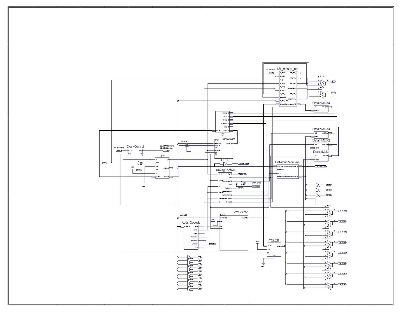
In honor of 10K+ views and especially for those who have helped me progress to this point, I post schematics, including Richard Herveille's I2C core.
Still working on drivers for it, but everything else is functioning with his core present , including the 2 external 4.7K pull-up resistors for SCL and SDA.
The FPGA has an internal pull-up function too, but I think I read they're only good for around 12K.
His documentation is abit tricky, so I am forced to interpret his VHDL, as far as his register assignments and that even is a little tricky.
His registers seem to change based on whether his I2C Master Core is reading or writing to a device, I'm not sure why... But I do intend to use his core for write only operation. So I think I have it straight.

This is the 6502SoC Top_Level Schematic so far (I'll try to fix the blockiness of the smaller fonts):
Image

Here are the modules from above:
Clock Control Module
TimingControl Module
Addr_Decode Module
DataOutRegisters
DataInMUXx
IO


Top
 Profile  
Reply with quote  
 Post subject:
PostPosted: Fri Apr 29, 2011 11:22 pm 
Offline

Joined: Mon Mar 02, 2009 7:27 pm
Posts: 3258
Location: NC, USA
Gonna hold off on working with the I2C Core at the moment, but I'll still leave it in. Need to get the PS2 Core up and running with a keyboard scan routine.


Top
 Profile  
Reply with quote  
Display posts from previous:  Sort by  
Post new topic Reply to topic  [ 224 posts ]  Go to page Previous  1 ... 11, 12, 13, 14, 15  Next

All times are UTC


Who is online

Users browsing this forum: No registered users and 13 guests


You cannot post new topics in this forum
You cannot reply to topics in this forum
You cannot edit your posts in this forum
You cannot delete your posts in this forum
You cannot post attachments in this forum

Search for:
Jump to: