Well, I've been learning quite a bit about NMOS the last few days, my previous experience has all been with CMOS.
I'm working on pre-optimizing the netlist in my software before the VHDL stage. I remove all duplicate transistors now, and I am working on spotting inverters and simple flops and replacing these with RTL code.
I'm pretty confident the VHDL netlist will work. There is still going to be quite a lot of manual work to tidy it up, for example replacing the PLA with case statements etc.
MikeJ
Visualizing the 6502
BigEd wrote:
But because it's at transistor level, and because there are bidirectional pass gates, you'd need the right kind of simulator...I don't know about verilog (and therefore about FPGA) - if you have good ideas about modelling bidirectional pass gates then we can try it.
Quote:
all the connectivity for pulldowns and the enhancement pullups are in transdefs.js, but the depletion pullups are in segdefs.h together with the layout-derived polygons.
fpgaarcade wrote:
I remove all duplicate transistors now, and I am working on spotting inverters and simple flops...
-
fpgaarcade
- Posts: 9
- Joined: 11 Nov 2010
"Mike. Those chips don't really have flip flops. That would be too expensive in terms of transistors. They mostly use clocked gates instead of flops. And they also use a lot of async latches."
Sure, but I see a lot of inverter pairs with transfer gates between them driven by the two clock phases. So, in these cases I can replace 6 transistors with a D flop. Doing this where possible rapidly brings the transistor count down to something I can cope with.
/Mike
Sure, but I see a lot of inverter pairs with transfer gates between them driven by the two clock phases. So, in these cases I can replace 6 transistors with a D flop. Doing this where possible rapidly brings the transistor count down to something I can cope with.
/Mike
I think I can understand the netlist description. Let's see if I'm correct:
The actual netlist is in transdefs. This files describes transistors in the format:
transistor_number,source_node,gate_node,drain_node
transdefs doesn't include depletion load transistors. They are described in segdefs. Here, the first field is the node number, and the second field is a plus or minus sign. A plus means there is a depletion load connected to this node. The rest of the line is not relevant for netlist purposes.

HiassofT wrote:
The link to the source code doesn't work (for me).
Ijor, yes, I think you've cracked the netlist code. I don't believe it's documented, but isn't too difficult. It's just a little annoying/odd that the pullup info is in a different file. Shouldn't be too difficult to transform into magic/irsim format. Irsim is probably the best bet as it's a switch level simulator.
I'd be very interested to see snippets of VHDL or verilog which can describe all the things we find on 6502. I'm presently trying to think of ways to speed up the javascript software simulation. Trying to move up from every transistor being bidirectional, perhaps up to logic gates or perhaps up to design-specific code describing each combinatorial cloud ought to be possible and worthwhile.
Cheers
Ed
We've just released another update to the simulator.
It's not a new feature, but it is possible to link direct to specific areas of the chip.
Here are the X, Y and S registers - bit 7. Showing two different flop designs, and also two types of control line - with clocked pullup and without.
Here's the ALU output latch, again just bit7. Also visible the overflow out and the distinct control for loading bit7 as opposed to bits 6 down to 0 - used in shifting.
Here's bit7 of the Accumulator
Finally, bits 7 and 15 of the PC.
Michael Steil will be presenting tomorrow at the CCC in Berlin, with a talk referencing the visual6502 project (and simulator)
In other related news, Peter Monta is working on an FPGA design which runs the 6502 netlist level simulation. He's steadily making it smaller and faster - it would be surprising if it compared favourably with a high-level model, but with this approach it should be possible to build FPGA replicas of historical 8-bit systems which are fully bug-compatible without needing to understand them in complete detail. (But by studying such an accessible model, one might be able to better understand the original.)
We have about a month of updates queued up which haven't yet been released, but the preview on github has them
BigEd wrote:
Michael Steil will be presenting tomorrow at the CCC in Berlin, with a talk referencing the visual6502 project (and simulator)
Last edited by BigEd on Sat Jan 01, 2011 10:36 am, edited 1 time in total.
Reverse Engineering the MOS 6502 CPU
Double update: Michael Steil's recent presentation on reverse-engineering the 6502 (at the 27th CCC in Berlin) is now up on YouTube in six 10-minute sections.
There's a huge round of applause as Balazs' giant schematic is shown!
(I think once or twice he credits to me some of Greg's achievements - a slip of the tongue. My contribution has been in tweaking and refining the Javascript interface to the simulator. Greg did all the chemistry, photography and polygon capture tools.)
... and now visualizing the 6800
BigEd wrote:
BigEd wrote:
... interested in the 6800, because I'd like to see what similarities and differences exist ...
See here for the simulation
- Attachments
-
- Visual6800 online simulator
Last edited by BigEd on Sun Oct 04, 2015 3:56 pm, edited 1 time in total.
I've posted some pictures on the visual6502 wiki, of the transistor netlist running on FPGA in some vintage hardware: atari 2600, apple IIe clone, vic20, c64.
(Well, partly the transistor level netlist: Peter Monta has written tools to convert much of the netlist to logic gates, and the rest is simulated. Ingo Korb did some clever fine-tuning of the clock delays. The FPGA is on an OHO module which fits directly into the vacant 6502 socket.)
This idea is good running up to about 1MHz so far. It's also passed the Wolfgang Lorenz test suite, with the exception of some unsupported opcodes. (There's more detail on the wiki page.)
Cheers
Ed
-
teamtempest
- Posts: 443
- Joined: 08 Nov 2009
- Location: Minnesota
- Contact:
Don't know if this link has appeared before; I just came across it today in one of the Commodore newsgroups:
http://www.archaeology.org/1107/feature ... p_cpu.html
http://www.archaeology.org/1107/feature ... p_cpu.html
-
ElEctric_EyE
- Posts: 3260
- Joined: 02 Mar 2009
- Location: OH, USA
Re: Visualizing the 6502
Not sure this is the best thread to mention this, but:
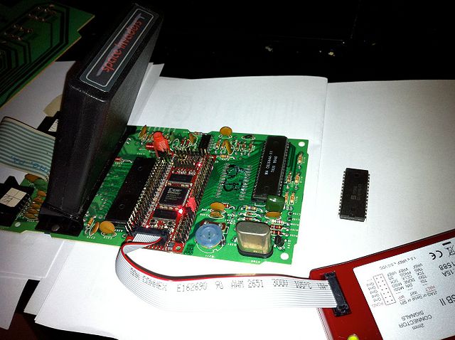
fpgaarcade (mike) has appeared to have finished his project!
fpgaarcade (mike) has appeared to have finished his project!
-
GARTHWILSON

- Forum Moderator
- Posts: 8773
- Joined: 30 Aug 2002
- Location: Southern California
- Contact:
Re: Reverse Engineering the MOS 6502 CPU
BigEd wrote:
Double update: Michael Steil's recent presentation on reverse-engineering the 6502 (at the 27th CCC in Berlin) is now up on YouTube in six 10-minute sections.
http://WilsonMinesCo.com/ lots of 6502 resources
The "second front page" is http://wilsonminesco.com/links.html .
What's an additional VIA among friends, anyhow?
The "second front page" is http://wilsonminesco.com/links.html .
What's an additional VIA among friends, anyhow?

Re: Visualizing the 6502
I think I found a small erratum in the visual 6502 data, though I doubt I'm the first to spot this:
t2730 pulls node 860 to ground, but node 860 is not connected to anything.
From the context I suppose it should have been connected to node 1163 clk1out.
See http://www.visual6502.org/JSSim/expert.html?find=806
Simulation-wise this makes no difference.
Edit: there is also another small unconnected component of "transistor: t1322 on gate: 866 c1: 9 c2: 657 vcc" e.g. http://www.visual6502.org/JSSim/expert.html?find=866 . This is around the op-push/pull row of instruction decoding logic, I'm not qualified to judge what was the intention here.