6502.org Forum  Projects  Code  Documents  Tools  Forum
It is currently Tue Sep 24, 2024 7:29 am

All times are UTC


Post new topic Reply to topic  [ 20 posts ]  Go to page 1, 2  Next
Author Message
 Post subject: Modular SBC
PostPosted: Fri Oct 22, 2010 4:28 pm 
Offline
User avatar

Joined: Fri Aug 30, 2002 9:02 pm
Posts: 1738
Location: Sacramento, CA
I have been toying with an idea of creating a simple, modular SBC based upon the DEC-1 memory decoder or similar device.

It would have a base board with power supply, clock oscillator, 65C02, 32K SRAM, 32K EEPROM that could be written in-system, the DEC-1, and a dedicated serial terminal port. This board could run all by itself.

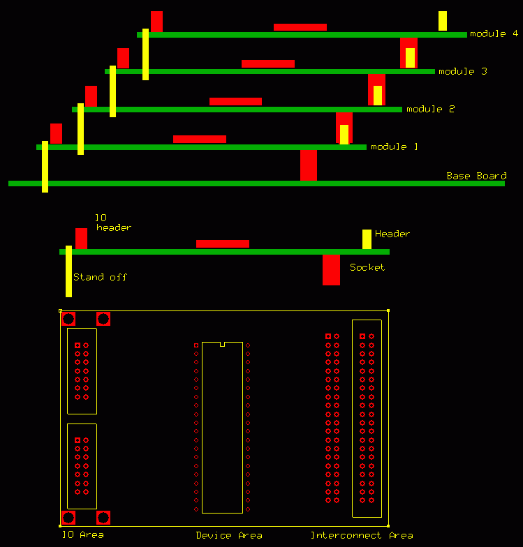
I would add an I/O connector that contained the data bus, A0-A3, the 4 IO Selects from DEC-1, PHI2, RW, IRQ, RESET, and power.

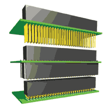
A daughter board would then be stacked on top of this connector with a matching female socket and standoffs. This board would have a staggered I/O connector facing up that would allow another board to be stacked on top.

The IO selects would be shifted between the bottom and top connector ( 2->1, 3->2, 4->3, +5v->4), similar to the 65SIB Slave selects, to allow for each board to be automatically addressed, based on its position in the stack.

This way, each builder could add his own suite of IO devices.

There could be modules with: 65C22, 65SPI, Mass storage, Video, sound , GP IO, etc. Each board would have 16 bytes of address space. That value could be increased to 32 or 64 bytes easily - at the expense of having more address lines on the IO connector. You can even have two or more of the same type module.

By limiting the stack to 4, there would be some control over the bus loading to keep performance moderately high. Again, if the consensus is to allow for more, that could be accommodated at the expense of increased bus loading.

Having the daughter boards staggered would allow for IO connectors to be easily accessed.

It would look something like this:
Image

A 65816 version of the base board could also be made and users could even create their own custom daughter boards using perfboard, as the spacing would be standardized on 0.1" centers.

All comments welcome.

Daryl


Last edited by 8BIT on Fri Oct 22, 2010 8:22 pm, edited 1 time in total.

Top
 Profile  
Reply with quote  
 Post subject:
PostPosted: Fri Oct 22, 2010 5:48 pm 
Offline

Joined: Thu Oct 21, 2010 1:40 pm
Posts: 22
Location: US
Reminds me of Arduino, the way "shields" can be stacked on top of a base unit (http://arduino.cc). Is that your inspiration?


Top
 Profile  
Reply with quote  
 Post subject:
PostPosted: Fri Oct 22, 2010 8:14 pm 
Offline

Joined: Wed May 20, 2009 1:06 pm
Posts: 491
I'm interested but I have limited knowledge of the Dec-1. I wasn't old enough and didn't have access to one.

I thought you might be able to use these enclosures if you design it to be compatible but it is an optional preference:

http://www.parallax.com/StoreSearchResu ... fault.aspx


Top
 Profile  
Reply with quote  
 Post subject:
PostPosted: Fri Oct 22, 2010 8:17 pm 
Offline
User avatar

Joined: Fri Aug 30, 2002 9:02 pm
Posts: 1738
Location: Sacramento, CA
No, I have not followed the Arduino's. I was just trying to find a way to make a system that was flexible and simple to implement for beginners while being functional for anyone. I like the idea of having a wide selection of I/O modules that can be combined easily.

Daryl


Top
 Profile  
Reply with quote  
 Post subject:
PostPosted: Fri Oct 22, 2010 8:21 pm 
Offline
User avatar

Joined: Fri Aug 30, 2002 9:02 pm
Posts: 1738
Location: Sacramento, CA
ChuckT wrote:
I'm interested but I have limited knowledge of the Dec-1. I wasn't old enough and didn't have access to one.


Hi Chuck,

The DEC-1 I was referring to is the memory decoder that I have created that takes care of the RAM, ROM, and IO device chips selection and gates the RW line with PHI2 for the memory WE and OE pins.

The clear enclosure you linked to is a great idea, thanks.

Daryl


Top
 Profile  
Reply with quote  
 Post subject:
PostPosted: Sat Oct 23, 2010 12:23 am 
Offline

Joined: Wed May 20, 2009 1:06 pm
Posts: 491
Daryl,

I have spent some free time over the space of two years looking up different components that I wouldn't mind seeing work with the 65C816. There is a new video chip being worked on that could possibly be interfaced to the 65C02:

http://www.parallax.com/Propeller2Featu ... fault.aspx

"Each cog has independent video generation hardware capable of VGA, Standard PAL/NTSC, and HD up to 1080p (at 30 Hz)."

"Main memory: 128 KB RAM(2) + 32 KB ROM planned"

The difficulty of the above chip is that it is 3.3 volts.

I have some other configurations (other chip suppliers) that I would only share privately but I want new hardware.

Chuck


Top
 Profile  
Reply with quote  
 Post subject: Re: Modular SBC
PostPosted: Sun Oct 24, 2010 9:54 am 
Offline

Joined: Mon Oct 16, 2006 8:28 am
Posts: 106
@8BIT

You might want to look at the PC-104 form factor. They're doing a very similar thing and you should be able to use their connectors for your bus.

Image


Top
 Profile  
Reply with quote  
 Post subject:
PostPosted: Sun Oct 24, 2010 3:04 pm 
Offline
User avatar

Joined: Fri Aug 30, 2002 9:02 pm
Posts: 1738
Location: Sacramento, CA
Thanks for that link. The tall female sockets look promising.

Daryl


Top
 Profile  
Reply with quote  
 Post subject: Re: Modular SBC
PostPosted: Sun Oct 24, 2010 3:49 pm 
Offline
User avatar

Joined: Fri Dec 12, 2003 7:22 am
Posts: 259
Location: Heerlen, NL
Hallo Daryl,
8BIT wrote:
All comments welcome.

To be honest, I'm not impressed. My reasons:
1- You need two connectors for every card you solder. Just try to imagine how you are going to solder the wires to those connectors, opposite off each other!
2- Using experiment boards normally means you can only solder at one side. How to solder the connector placed at the solder side?
3- Using PCBs means they have to be double sided as well = more costs.
4- Video cards, I/O cards, etc. have connectors at the front. Just try to put the whole in a box with those connectors at the front. Better, try to find a box for it at all!
5- Knowing Murphy, it is always the card in the middle that needs to be taken out, replaced or what ever!

Using a backplane means:
- you only need one connector. Yes, the backplane needs one as well but that one is "reusable".
- The depth is always the same. So connectors can pop out of the front of the box.
- Because the depth is the same, you can get standard boxes. There may be a limit to the width.
- Replacing/taking out cards is done in a few seconds.
- Regarding PC-104, that is more interesting, but only for PCBs, not for wired projects.

My honest oppinion, no offense meant and I'm always open for new ideas :)

_________________
Code:
    ___
   / __|__
  / /  |_/     Groetjes, Ruud
  \ \__|_\
   \___|       URL: www.baltissen.org


Top
 Profile  
Reply with quote  
 Post subject:
PostPosted: Sun Oct 24, 2010 5:11 pm 
Offline
User avatar

Joined: Fri Aug 30, 2002 9:02 pm
Posts: 1738
Location: Sacramento, CA
Ruud,

Thanks for the feedback. You have some excellent points. I know the expense would be more using two connectors and double-sided boards.
I had considered using a one-piece female socket with tall posts (wire-wrap length) that could be stacked vertically. I like the idea of the auto-addressing scheme two connectors would provide, but that may be easily replaced with a simple jumper block instead.

thanks

Daryl


Top
 Profile  
Reply with quote  
 Post subject: Re: Modular SBC
PostPosted: Sun Oct 24, 2010 5:22 pm 
Offline

Joined: Sat Jan 04, 2003 10:03 pm
Posts: 1706
Ruud wrote:
5- Knowing Murphy, it is always the card in the middle that needs to be taken out, replaced or what ever!


PC/104 cards suffer from this malady, too.

However, backplanes as Ruud uses the term have several problems of their own:

Quote:
- you only need one connector. Yes, the backplane needs one as well but that one is "reusable".


You quite often need big connectors, either in terms of pins (to accomodate as many future expansions to the bus as you can) or in terms of physical size (to accomodate mechanical registration/alignment errors). You also need mechanical support separate from these connectors, since they represent a single point of flexure, and thus, the primary cause of failure.

The stacked PCBs have the advantage that weight is distributed evenly, and with a wide berth, there is little to no flexure to wear out the pins or surrounding plastic. Additionally, you can put new buses on extremity cards, allowing for future bus capabiilities without requiring a large number of pins on the basic bus connector. Note that PC/104 now has a PCI bus connector standard, located right next to the ISA bus connector, which allows the use of either PCI or ISA-based cards in the stack. By placing all PCI cards next to each other, they control PCI bus timing characteristics. So, you tend to have a stack of ISA-cards on top of or beneath a stack of PCI cards. See http://eri.ca.sandia.gov/eri/howto.html

Quote:
- The depth is always the same. So connectors can pop out of the front of the box.


The disadvantage is, strangely, that the depth is always the same, meaning small peripherals must be mounted on PCBs that are, frankly, way bigger than necessary, which adds immensely to the cost of the project. I'd wager PCB fabrication costs often dwarf the costs of the parts put on it (since you pay by the square inch/cm), so it behooves anyone designing a standard bus to enable a variety of board sizes.

This problem isn't limited to just the cards, though -- attempting to resize the average enclosure box to accommodate increasingly smaller designs then results in the situation where larger cards cannot fit, which means the user must either find, design, or purchase a smaller card that does the same, or simply give up in frustration.


Top
 Profile  
Reply with quote  
 Post subject: Re: Modular SBC
PostPosted: Sun Oct 24, 2010 7:49 pm 
Offline
User avatar

Joined: Thu May 28, 2009 9:46 pm
Posts: 8392
Location: Midwestern USA
kc5tja wrote:
The disadvantage is, strangely, that the depth is always the same, meaning small peripherals must be mounted on PCBs that are, frankly, way bigger than necessary, which adds immensely to the cost of the project. I'd wager PCB fabrication costs often dwarf the costs of the parts put on it (since you pay by the square inch/cm), so it behooves anyone designing a standard bus to enable a variety of board sizes.

This problem isn't limited to just the cards, though -- attempting to resize the average enclosure box to accommodate increasingly smaller designs then results in the situation where larger cards cannot fit, which means the user must either find, design, or purchase a smaller card that does the same, or simply give up in frustration.

This is no different than what PC designers face. Case in point: the venerable 3Com 3C905 NIC. When it first appeared it was a quarter-length, full height PCI card. In its final iteration, the PCB itself was substantially smaller that the original, but with identical functionality. To some extent, the use of the separate mounting bracket to attach the card to the chassis rear bulkhead mitigates the size variations. However, what can't be mitigated is the positioning and size of the connector on the motherboard. You can only get adjacent connections so close and then assembly problems ensue.

I have to agree with Ruud that the backplane approach would work better with what Daryl has in mind. One problem I foresee with Daryl's approach is the issue of mechanical tolerance stack-up (no pun intended) as the number of boards in use increases. Small variations in connector and pin header positioning could make it difficult to impossible to to attach the Nth card if N is more than a handful.

Something else to consider is cooling. Most of the parts we use don't produce much of heat, when considered individually. Stack up a bunch of them, though, and who knows what will happen. Also, consider that CPLDs and FPGAs tend to get pretty toasty and can go wacko if not adequately cooled.

All of the above, of course, is opinion, although there is some experience in there as well.

_________________
x86?  We ain't got no x86.  We don't NEED no stinking x86!


Top
 Profile  
Reply with quote  
 Post subject: Re: Modular SBC
PostPosted: Sun Oct 24, 2010 9:24 pm 
Offline

Joined: Sat Jan 04, 2003 10:03 pm
Posts: 1706
BigDumbDinosaur wrote:
This is no different than what PC designers face.


It's actually quite different, and your response to me proves my point perfectly. Standard backplane cages place the connector at the far-end of the PCB, as far away from the user interface bulkhead as possible. This makes inserting and removing cards by teen-aged level-1 NOC technicians an effortless and error-free process. It also means you don't have to disassemble the chassis to swap out cards.

In contrast, PC expansion cards have the connector adjacent to the bulkhead. This arrangement has virtually the opposite set of advantages and disadvantages: to swap out a card, you need to disassemble the chassis, which implies powering the system down. Additionally, you need to have some wit about you to perform the procedure, lest you risk fracturing the motherboard (no rear reinforcement of the board), shorting out the motherboard (where did that damn screw go again?), and god help you if your box is liquid cooled -- don't spill anything while you're swapping in that new video card you just spent a grand on!

While it remains true that you can shrink the board only so far (it has to be at least large enough to fit the connector), it's also true that the lengths of PCBs can vary significantly, at least in one dimension (and usually two dimensions -- the smallest NIC I ever installed was 0.75 inches high after inserting into the slot), and it's generally true that you can say that a board can be as large as required to fit the circuitry. This simply cannot happen with a VME-type backplane arrangement, where both vertical AND horizontal dimensions remain fixed, leading designers to either:

* place small circuits on fixed-sized PCBs, leading to a higher-than-necessary minimum card fabrication cost,

* place large circuits on multiple cards, each taking up an otherwise potentially useful slot. You then need to use a front-plane or mezzanine bus to connect them. This is like nVidia's SLI bus to bridge multiple video cards into a kind of graphics cluster.


Top
 Profile  
Reply with quote  
 Post subject:
PostPosted: Mon Oct 25, 2010 2:13 am 
Offline
User avatar

Joined: Fri Aug 30, 2002 1:09 am
Posts: 8514
Location: Southern California
A possibility for stacking the boards is hinged standoffs like these (available at Mouser) which come in different heights. When the board-to-board connectors get long, it becomes difficult to separate them without damage, especially if the boards are parallel to each other. It takes a lot of force, and then if one end suddenly comes out before the other, you may end up with bent pins. (It's a little easier to control and avoid this if the boards are at right angles to each other; and of course a card cage with card guides completely eliminate the danger.) With the hinged standoffs, putting the connectors at the edge opposite the one with the hinged standoffs guarantees that the connectors will be held straight as they are separated. Another possibility is short ribbon cables connecting the boards on the hinged end, even allowing opening up the sandwich during operation to probe something if necessary for example. This also makes it easy to adjust the height if a particular board has taller parts for example, as different standoff heights are much more available than different connector heights. I don't normally use shrouded headers with ejector hooks for the ribbon cable connectors, but they would be beneficial if you're making this for others, to facilitate unplugging them without bending any pins.

If you turn the stack sideways (so boards are vertical), the convection works just as well regardless of the thickness of the stack, so heating should not be an issue.


Top
 Profile  
Reply with quote  
 Post subject:
PostPosted: Mon Oct 25, 2010 12:16 pm 
Offline
User avatar

Joined: Fri Aug 30, 2002 9:02 pm
Posts: 1738
Location: Sacramento, CA
I like the idea of using the ribbon cable for a "cheap" backplane. This would also make it so there's 1 connector on the boards - making perfboard construction easier and single layer pc board designs possible.

I can just add a jumper block to allow the chip selects to be optioned instead of using the auto config format.

This also allows for all the board edges to be in the same plane for those wanting to place it in an enclosure.

Daryl


Top
 Profile  
Reply with quote  
Display posts from previous:  Sort by  
Post new topic Reply to topic  [ 20 posts ]  Go to page 1, 2  Next

All times are UTC


Who is online

Users browsing this forum: Google [Bot] and 92 guests


You cannot post new topics in this forum
You cannot reply to topics in this forum
You cannot edit your posts in this forum
You cannot delete your posts in this forum
You cannot post attachments in this forum

Search for:
Jump to: