Bidirectional buses are a PITA because they can violate timing constraints that synthesis languages depend on for correctness. Lots of loading and long lead lengths (even on chip) can result in unpredictable propagation delays.
Separating the input and output buses allows you to use all point-to-point links, which are, at once, easier for the synthesis software to route, easier to analyze timing for, and absolutely guarantees a circuit where you cannot accidentally short something out. A "bus" is constructed by logically ORing (or, if active low, ANDing) the relevant signals. For example, if you were to replicate a Commodore 64, you'd form its backbone bus by ORing D0_CPU_O, D0_VIC_O, D0_SID_O, D0_CIA1_O, D0_CIA2_O, and D0_RAM_O to a single D0_BUS_I. That way, bus contention only yields incorrect results, never a short circuit, and you always know that the bus delay is a single gate (the OR gate). If I recall correctly, there is a great explanation of this in the Wishbone bus specifications.
Project: Digital Fuel Injector Pulse Width Analyzer
-
ElEctric_EyE
- Posts: 3260
- Joined: 02 Mar 2009
- Location: OH, USA
@kc5tja, I thought you said you didn't know about FPGA's?!
@myself. Ok, so the last pic I posted read from banked ram I tried to come up with a pattern to put into ram then send it to the display. The intended pattern didn't work, but the overall test was a success. The displayed data was 100% repeatable...
I realized today, all this display wants is 3 consecutive bytes representing 18 bit RGB data. So I decided to do a clear screen with blue (#$00,#$00,#$FF) to determine what I was working with. Looking at the last pics you'd think it's 640Hx480V. Well what I found out today, the way the display is positioned in my pic (&BDD's heh) is that Horizontal is actually 512 and Vertical is 640!
The init values I got from NHD are set for 480x640 or I thought 640x480. The display Ram can be rotated but still, 512 is no 480!
ElEctric_EyE wrote:
@kc5tja, I thought you said you didn't know about FPGA's?!
Though, come next year, as a Christmas present to myself, I'm looking to change that.
-
BigDumbDinosaur

- Posts: 9426
- Joined: 28 May 2009
- Location: Midwestern USA (JB Pritzker’s dystopia)
- Contact:
kc5tja wrote:
ElEctric_EyE wrote:
@kc5tja, I thought you said you didn't know about FPGA's?!
Though, come next year, as a Christmas present to myself, I'm looking to change that.
x86? We ain't got no x86. We don't NEED no stinking x86!
-
ElEctric_EyE
- Posts: 3260
- Joined: 02 Mar 2009
- Location: OH, USA
-
ElEctric_EyE
- Posts: 3260
- Joined: 02 Mar 2009
- Location: OH, USA
OK, so when I said the bidirectional bus was working inside the FPGA, it was/IS working for the single 7-bit port that controls the upper banked addresses A14-A20, to the 2Mx8 RAM. The software is successfully performing INC on the SRAM Bank Register... I had intentions of using a building block approach to make more ports since this one worked...
But when I needed another port to read from the 'PS2 core' keyboard interface I put in the FPGA, everything went to crap. Got tons of errors. Bidirectional errors. Even though the PS2 core synthesized perfectly and I easily made a symbol...
So I went back to the basics this morning, and came up with this: viewtopic.php?t=1665 , after Andre's post.
I may just relax awhile and try to learn a little more about FPGA's while at the same time working out some more software routines for the display since everything is working so nicely as far as the display & banked RAM is concerned. But, I am at a crossroads. I'm pretty sure I could get the internal registers I need to work if I rewire in the CPLD I have in mind, a 100-pin QFP Coolrunner II XPLA3. But then the PS2 core wouldn't fit into it. I know it will fit into the XC2S15, even though all by itself, the PS2 core uses 50% of the FPGA resources. But if I don't have the PS2 interface I am stuck reprogramming the EEPROM after every simple modification.
......
I've noticed on most if not all FPGA development boards, they have a CPLD onboard to go hand in hand with the FPGA. I'm starting to think that's what I may need here as well. Put all the cores (PS2, IDE, USB, I2C) into 1 FPGA with separate Input data buses and Output data buses, and then bring them all together at the CPLD to interface to the 6502 and memory.
Once again, starting from scratch! But I may just relax awhile and experiment with what I've got...
-
ElEctric_EyE
- Posts: 3260
- Joined: 02 Mar 2009
- Location: OH, USA
Got the FPGA (XC2S15) working using multiple bidirectional ports internally. The progress made was posted in the link above. I'm forgetting about using CPLD's for now...
Working so far:
1) ROMBank and RAMBank ports working bidirectional inside the FPGA, meaning 6502 INC & DEC commands can be used on these registers.
These ports control upper addresses to the 512K EEPROM and the 2M SRAM.
2) The "on the fly" Phase 2 clock (2.5 or 20MHz) switching circuit for EEPROM to SRAM copying.
In Situ:
3) The PS2 Core, PC keyboard interface, (not working yet) but it still fits. Now up to 75% usage of IOB's...
Made by Daniel Quintero, it's available @ Opencores.org. Thankfully, it uses the Wishbone Interface, which I'm presently reading up on... Others have said Wishbone is easy to interface to the 6502. I'll post my progress!
-
ElEctric_EyE
- Posts: 3260
- Joined: 02 Mar 2009
- Location: OH, USA
Man was that easy!
I did a "quickie" test with a simple loop that reads wb_dat_o (wishbone data out) and writes the same value to the R, G, & B for the display. So it will only display black for 0,0,0 and white for $FF,$FF,$FF. Typing on the keyboard produced expected shades.
The PS2 core info on opencores.org states that it was based on info from this site:
http://www.beyondlogic.org/keyboard/keybrd.htm
Although the core is written in VHDL here is what the wishbone symbol looks like:
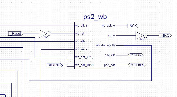
wb_clk_i is the 20MHz Phase 2.
wb_stb_i is an active high chip select.
wb_we_i is write enable.
A0 selects the data register or the status register.
irq_o can be set to be active on different conditions by the status register.
wb_dat_o is the latched data. Last key pressed remains on the bus.
Sending data to the keyboard doesn't seem to be working yet. Trying to light up num lock, caps lock, and scroll luck, by sending #$ED, then #$07.
I did a "quickie" test with a simple loop that reads wb_dat_o (wishbone data out) and writes the same value to the R, G, & B for the display. So it will only display black for 0,0,0 and white for $FF,$FF,$FF. Typing on the keyboard produced expected shades.
The PS2 core info on opencores.org states that it was based on info from this site:
http://www.beyondlogic.org/keyboard/keybrd.htm
Although the core is written in VHDL here is what the wishbone symbol looks like:
wb_clk_i is the 20MHz Phase 2.
wb_stb_i is an active high chip select.
wb_we_i is write enable.
A0 selects the data register or the status register.
irq_o can be set to be active on different conditions by the status register.
wb_dat_o is the latched data. Last key pressed remains on the bus.
Sending data to the keyboard doesn't seem to be working yet. Trying to light up num lock, caps lock, and scroll luck, by sending #$ED, then #$07.
-
ElEctric_EyE
- Posts: 3260
- Joined: 02 Mar 2009
- Location: OH, USA
Today I was able to update a few critical routines I had written for the old 320x240 display for the new 640x512 display. Routines like 2-digit 8 bit hex to 3 digit decimal conversion (thanks to 6502.org!), and character plotting. Character plotting is MUCH easier with this new display. Now that I'm checking out Newhaven's site for the link, I see they have a new 7" 800x480 display for $86! $20 cheaper with the same controller. Same controller means just a few simple variable changes... Very tempting!
So anyway, I made a simple routine to monitor the keyboard, and mapped a table for keystrokes, and displayed the decimal value for keystrokes and the resultant character.
Turns out Daniel Quintero's PS2 core has not been completed. It's good for translating all keypresses into individual codes. But it does not activate LEDs, and there's no way to do a momentary shift + keypress for a capital letter or the symbols above the numbers. One big positive is that the code is very short and I may end up still using it as I really only need very basic input for assembly input (eventually).
Another core I found today in opencores.org SVN repository was made by John Clayton and Miha Dolenc. It's documented very well, says it supports turning on LEDs, has "shift trapping" and more...
I hope it fits into the XC2S15. Will find out soon!
-
ElEctric_EyE
- Posts: 3260
- Joined: 02 Mar 2009
- Location: OH, USA
I'm going to stick with Daniel Quintero's PS2 keyboard Core... It's very simple and it works, and especially since I hit my limit trying to fit an I2C core into the same XC2S15.
I'll try to use the status register to "trap" the shift keys...
Which ultimately means, I will work with my current board to develop a few more software routines. They will be mainly graphic routines to help display characters/lines/boxes, and also a keyboard buffer routine to help control things.
I have a video posted here to show the basics and the proof of what I've had so far. I need to post another video soon, as this one does not show the PS2 Core...
One idea I have for displaying characters, is to define each character with 2x8 bit data. For each character displayed, an 8 bit ascii is sent first, then another 8 bits is sent to the PLTCHR routine which defines the following:
1 bits specify 2 fonts,
3 bits specify 7 different sizes (there is no "zero" size)
4 bits select 16 colors (according to C64 specs here: http://unusedino.de/ec64/technical/misc/vic656x/colors/).
Soon, I'm going to have to make a jump to a larger 144-pin XC2S100 Spartan II FPGA. It WILL fit the PS2 Core and the I2C core which will control this frequency synthesizer.
Although when I make this jump, it will be a big one! No more adapter sockets! It will be time to put this foundation on a board! All unused XC2S100 pins go to an expansion connector...
I am tempted to be reckless and jump a few steps ahead and put one of the fine 6502 Cores reviewed here, along with the PS2 and I2C cores, into a 208-pin Spartan 3 FPGA. I'm not quite there yet. If I did do this, I would have to wirewrap it.
Edit: Changed character attributes
Last edited by ElEctric_EyE on Tue Jan 04, 2011 1:44 pm, edited 1 time in total.
-
ElEctric_EyE
- Posts: 3260
- Joined: 02 Mar 2009
- Location: OH, USA
Plans have changed a little...
I am abandoning the 6502. Consider me a 65816 "convert". I was hellbent on the 6502 because I was used to programming it. But doing some of the 16 bit math for the graphics routines are very cumbersome (i.e. time consuming). Whilst following another thread, just a few commands/features were discussed which finally changed my mind for good about the '816. It was always in the back on my mind however...
I will be scrapping this board to make room for another project. Will make a video before scrapping, once I'm done with the final 6502 hex-dump routine. I will be able to change banks, font colors, font sizes, and dump the hex data onto the display...
Not much will change in terms of layout for this new stage of the PWA project. I will be wiring in the FPGA PROM this time, and the I2C oscillator mentioned earlier. (I was considering the PCA9538, however, is not an I2C controller. Closer look at the datasheet showed it to be an I2C expander). No matter now, there will be an I2C core inside the larger FPGA!
Wirewrapped IC's on a new vectorboard will be:
Spartan 2 XC2S100 144-pin QFP
XCF02 FPGA Config PROM
W65C816 44-pin PLCC (where's our QFP?!)
2Mx8 SRAM
512Kx8 EEPROM
DS1085 Prog. Osc.
An 8-bit ADC
Also, I'll be using NewHaven's new 800x480 display w/touchpanel.
A few adapter sockets need to be purchased, along with the 65816, ADC, and a new vectorboard. Everything else is in the staging area!
--------------------------------------------------------------------------------------
Ordered the new 800x480 display and the Vectorbord today (1/5/11)...
--------------------------------------------------------------------------------------
Ordered the 144-pin QFP adapter sockets from epboard (1/7/11)...
--------------------------------------------------------------------------------------
Once again plans have changed on ----------------------(1/12/11):
The Spartan II is no longer needed for 5V input compatibility. The Spartan II 5V input tolerance ability has been sacrificed for Spartan 3 distributed RAM/ROM ability. The 144-pin adapter socket will be put to better use utilizing this Spartan 3. Will also be trying to fit the EEPROM into the Spartan 3, hence the question mark (?) after the EEPROM part. It most likely will be replaced by a 2Mx8 48-pin TSOP 3.3V Flash.
Spartan 3 XC3S200 144-pin QFP
XCF02 FPGA Config PROM
W65C816 44-pin PLCC
2Mx8 10ns SRAM
512Kx8 EEPROM?
DS1085 Prog. Osc.
An 8-bit ADC
__________________________________________________________________________________________________________________________
It has changed once again (05/05/2011) based on what I have learned from the 6502SoC hardware:
Spartan 6 XC6SLX9-2 144-pin QFP
XCF02 FPGA PROM
2Mx8 70ns Flash
DS1085 I2C Programmable Oscillator
DS1818 3.3V EconoReset w/pushbutton
An 8-bit 2-input MUX'd ADC