The problem is that java script simulator does not have labels on each gate. I can't tell where data is flowing through components from data bus.
I'm continuing to add to the list of named signals, and I'm sure we'll do something to make a user interface which helps in using them. Presently I'm modifying the javascript on the fly (the browser offers a javascript console, one can change the code there, invoke functions, and take a plain text log. It's a command line!)
But, this is open source, so anyone can help. It's not so hard to teach yourself how to read the layout, if you're so inclined.
...The problem is that java script simulator does not have labels on each gate...
I'm adding new labels as we speak: I think I now have labels for all the internal busses and most latches. My updates will hopefully be published before long - we'll probably be setting up a shared source control system.
ElEctric_EyE wrote:
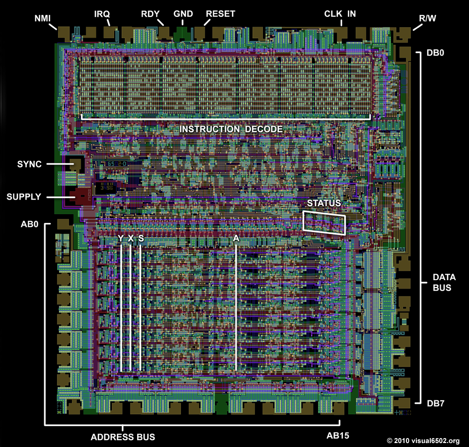
I could sort of tell where the A0-A15 and D0-D7 pads were.... This should help...: http://visual6502.org/images/6502/6502_pad_annot_07.png . My question is, and this may be off-topic, what is the device betwixt D3 and D4?
Looks like a test structure for me: those mini-pads don't get bonded out in production, but some parameter like diffusion resistance. There are some other test structures and mini-pads over by A0. It's more visible in the die shot
In the on-chip photo, you can see traces leading from the guts of the chip to the "test pads." I'm thinking it's not a test pad, but perhaps an on-chip decoupling capacitor.
I don't think there is a connection: there are some structures (perhaps protection structures) which belong electrically to the two adjacent D pads. Greg has (much!) higher resolution photos, of course, which I expect will be available in due course.
6502 schematic in PDF format shows thousands of transistors. Are they field effect transistor? Are they two different transistors? What is the difference between white rectangle and white line?
Every transistor would be an N-channel, enhancement-mode MOSFET transistor. Some transistors might be physically larger than others (e.g., smaller transistors have larger resistance, and thus excel as smaller versions of pull-up resistors). However, in principle, they're all the same kind of transistor.
If I'm seeing the same thing you are, white lines correspond to metal wires, while brownish lines are polysilicon lines. The dots are vias where different layers of the chip connect.
Hang on a sec - Bryan is looking at the big schematic. I suspect Samuel may be looking at layout.
Yes, they are all FETs, and all n-channel.
But, the transistors with a heavy dark line are depletion-mode FETs, which are used to pull up the output of almost all logic gates - with a single enhancement-mode pull-down, you've got an inverter; with two, you've got a NOR or NAND depending on whether they are in parallel or in series. You'll see some very complex gates in there - and the PLA columns can be seen to be NOR gates too.
You can more or less think of depletion-mode as resistive pullups. For large drivers - the drivers for the pads and for the datapath control signals - the pullup is an enhancement-mode device, which gives better drive and lower power consumption, but pulls up to a lower final voltage.
Because you have thousands of logic gates with resistive pullups, nMOS chips use a lot of power relative to CMOS. But the fabrication is simpler, and you have half as many transistors.
Cheers
Ed
Last edited by BigEd on Sun Sep 19, 2010 6:13 am, edited 2 times in total.
