
The main idea behind buying the Godil is replacing the original 6502 of my Commodore VIC-20 and adding extra opcodes/features the original 6502 doesn't have. Another idea I had was expanding my VIC-20 with an ISA bus, enabling me to use various PC cards. The Godil could give extra address lines etc. to simplify the design.
In fact I have played with the idea of replacing an 8088 with a 6502 but that turned out to become quite a difficult project, seen from the point of hardware.
Now the weird idea that just popped up: what about replacing the 8088 with the Godil and giving it a 6502 core? As said just an idea, but I really like it :)
More uses for the Godil
More uses for the Godil
Code: Select all
    ___
   / __|__
  / /  |_/     Groetjes, Ruud
  \ \__|_\
   \___|       URL: www.baltissen.org
-
BigDumbDinosaur

- Posts: 9426
- Joined: 28 May 2009
- Location: Midwestern USA (JB Pritzker’s dystopia)
- Contact:
More uses for the Godil
What, pray tell, is a Godil? Is this some sort of terrestrial creature found only near the dikes of Holland? 
x86? We ain't got no x86. We don't NEED no stinking x86!
-
nichtsnutz
- Posts: 9
- Joined: 03 Feb 2010
Hello all,
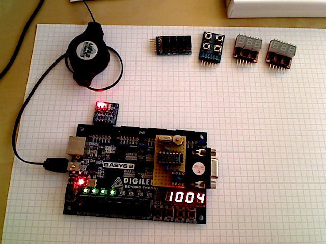
this is my first post here,so I would like to introduce myself a bit first.My name is Vassilis and I am from Germany.My hobby interests are primary the Atari 8bit computer and the Atari consoles A2600 and VC7800.All of them have a 6502 based CPU.I am exploring a little bit their hardware function and am building small extensions for them.I am also interested in the use of a T65 fpga core to replace the atari Sally CPU,so I am reading here very interested about the progress of the 6502 fpga thread and the tube project.I have only a small progress on the topic,I have compiled the T65 core and have use it on a "basys2" Xilinx board from digilent and I am able to single step small prorgams that are hardcoded in VHDL.The Adressbus is shown on the onboard 7-segment leds.My progress is slow,as I have to learn much about VHDL and hardware design.My next steps will be trying to use a 2k blockram to load a program over rs232 or the digilent adept suit,whichever will be easier.
Thank you for maintaining this nice forum,
Vassilis
@BigDumbDinosaur: A GoDIL is a FPGA module that can replace a 40p DIL Chip.The user BigEd has posted a Photo of it in the "6502 FPGA" thread on the last post.
Herzlich willkommen!
You were faster then me, thanks!
nichtsnutz wrote:
@BigDumbDinosaur: A GoDIL is a FPGA module that can replace a 40p DIL Chip.The user BigEd has posted a Photo of it in the "6502 FPGA" thread on the last post.
Code: Select all
    ___
   / __|__
  / /  |_/     Groetjes, Ruud
  \ \__|_\
   \___|       URL: www.baltissen.org

Welcome, Vassilis!
This is what I should do - I'm pretty sure I had a T65 running nicely on one of the OHO modules, but I haven't yet successfully interfaced it. Using LEDs would be an easy way to see what's happening (or not happening.) The OHO LEDs are serial-connected, so I need to do a little plumbing to make use of them.
(I could see SYNC running at various frequencies depending on the test program, so it was alive. The test program was a few bytes hard-coded into the FPGA.)
I believe the best version of T65 is the one from pacedev (even though the one on fpgaarcade claims to be the latest - I'm sure it was the latest, at one time.
(I recently learnt of another vhdl 6502 core.)
Cheers
Ed
nichtsnutz wrote:
The Adressbus is shown on the onboard 7-segment leds.
(I could see SYNC running at various frequencies depending on the test program, so it was alive. The test program was a few bytes hard-coded into the FPGA.)
I believe the best version of T65 is the one from pacedev (even though the one on fpgaarcade claims to be the latest - I'm sure it was the latest, at one time.
(I recently learnt of another vhdl 6502 core.)
Cheers
Ed
-
nichtsnutz
- Posts: 9
- Joined: 03 Feb 2010
Hello BigEd,
I have made a picture of my small setup that I use to play with the T65 core.For different reasons I unfortunately have not made big steps until now.I also single step through hardcoded programs.I use the T65 version from fpgaarcade.
I have tried to understand a little how the T65 core works.
The big parts are the ALU and the MCODE modules.Both are pure combinational modules as far as I understand.
I have also commented the MCODE module with the instructions.It is very difficult to find something in this *very big* "case ... when" statement.
The main signal that lets all things flow is the "MCycle" in the main loop.Every instruction defines a "LCycle" for last cycle(?) and depending on the IR (instruction register) and the "MCycle" several control signals and multiplexers are set.
I have not understood where PHI1 and PHI2 are! Every time I do one step, one PHI1/PHI2 cycle is done.I thought I would have to do two steps for one cycle because the 6502 is working on both edges of the clock!?
Anyway,first I have to connect two more 7 segments from OHO so that I can also see the input and output data busses.I would also like to be able to see the MCycle and LCycle signals for the current instruction.OHO has some example code to control the modules.
The onboard switches and leds I would like to have them as I/O ports.
I will also take a look at the other 6502 cores but personally I will stay with the T65 because I have already spend much time with it.
Also the work you are doing with the visual6502 is very interesting.I cannot run the program,I only have the windows explorer and it is not working,I do not know why,I have no knowledge in java.
Ok,this is much work to be done!
Greetings,
Vassilis
Hi Vassilis
good to hear of your progress and see your setup.
visual6502 is taking all my time at the moment. It's javascript, not java, but you do need a modern browser. It's possible IE9 might work. Chrome works well- it's an easy download/install and very uninvasive. You don't have to lose your normal browser.
As for clocking, the modern convention is that everything uses edge-triggered flops, and all the combinatorial logic sits between the flops. The 6502 used transparent latches, with two non-overlapping phases, and was able to place logic between any pair of latches. It's harder to design things that way, but it offers more freedoms. The result: people probably had to work quite hard to code up in a modern design style, but they did it.
I think the main part of chip behaviour - visible from the pins - which cares about clock phases, would be the databus being undriven during phi1. That's a simple fix to the pad tristates. (It might be that the interrupt inputs care about the clock phase, but it would be difficult to see that difference in practice.)
Maybe you can share your commented T65 code and it could be merged back ... somewhere? I'd be interested to see it, anyway.
Cheers
Ed
BigEd wrote:
As for clocking, the modern convention is that everything uses edge-triggered flops, and all the combinatorial logic sits between the flops. The 6502 used transparent latches, with two non-overlapping phases, and was able to place logic between any pair of latches. It's harder to design things that way, but it offers more freedoms. The result: people probably had to work quite hard to code up in a modern design style, but they did it.
Quote:
(It might be that the interrupt inputs care about the clock phase, but it would be difficult to see that difference in practice.)
RDY is an important signal to watch out for, since if it's asserted close enough to the phase-2-to-1 transition, it will not be recognized and can introduce accidentally introduce a wait-state.
-
nichtsnutz
- Posts: 9
- Joined: 03 Feb 2010
Hello Ed,
thank you for the explanations!
Sharing the code is no problem.I have only made small changes:
- Removed some unused signals that were generating warnings.
- Changed binary opcodes like "00011000" to x"18" to be better readable.
- Added small comments to the opcodes when they were not there to make this huge "case IR(...) is" statement more readable.
But I can not upload anything in this forum.If you give me an email address I can send the modified source to you.But be awere that this is a work in progress so things will change...
Greetings,
Vassilis