"star" distribution, i.e. from the center outwards. I use this principle when wire-wrapping power connections.
More recently, I've been applying this principle to data bus and address lines too. Am I correct in doing so?
SRAM trouble
-
ElEctric_EyE
- Posts: 3260
- Joined: 02 Mar 2009
- Location: OH, USA
It seems that fixing the power supply on the CPU board has fixed my problem! Yesterday it ran for over an hour already, and it's been running for almost an hour now without issue.
It always amazes me. A power supply issue on the CPU board with its drivers only makes a difference if on the BIOS board a larger RAM is used...
Pity that it's a a lesson already learned - I'm doing a much better board design concerning power supply these days than I did then. So it's a sin of the past that seems to have haunted me here... ;-)
BTW: the replacement RAMs I ordered, although the datasheet on the web site said something different, are of the very same type again....
Thanks for your help folks - sometimes it's enough just to discuss a problem to get on the right track.
André
ElEctric_EyE wrote:
"star" distribution, i.e. from the center outwards. I use this principle when wire-wrapping power connections.
More recently, I've been applying this principle to data bus and address lines too. Am I correct in doing so?
More recently, I've been applying this principle to data bus and address lines too. Am I correct in doing so?
When going to higher frequencies (or DRAMs :-) I am now more inclined to actually do some bus design: single signal line, feed from one side through small series resistor, terminator resistors, and only very short connects from this bus line to each receiver.
Maybe "star distribution" works with appropriate termination on each of the rays, and maybe even series resistors at the beginning of each ray (making it a variation of my "bus design".)
But others here are more experienced in these matters than I am :-)
André
-
GARTHWILSON

- Forum Moderator
- Posts: 8775
- Joined: 30 Aug 2002
- Location: Southern California
- Contact:
-
ElEctric_EyE
- Posts: 3260
- Joined: 02 Mar 2009
- Location: OH, USA
Glad to hear you fixed the problem! Heh, a solution to problem revisited is almost never forgotten.
In the past, when wiring data and address connections between CPU, SRAM, EPPROM and peripherals, I used to hop from CPU, to SRAM, to EPROM, etc., i.e. "tree" distribution. Now I wirewrap power, data, and address from CPU to SRAM, CPU to EEPROM, etc. Common sense tells you if you can keep all these IC's around the CPU, the distances would be shorter, but... Andre picked up on something here. I too am unfamiliar with electromagnetic workings inside the wire, skin effect, reflections, etc. I ask now because soon I will have to have PCBs made, very soon. I would like to get it right the first time. This could be a good thread to continue this topic?
In the past, when wiring data and address connections between CPU, SRAM, EPPROM and peripherals, I used to hop from CPU, to SRAM, to EPROM, etc., i.e. "tree" distribution. Now I wirewrap power, data, and address from CPU to SRAM, CPU to EEPROM, etc. Common sense tells you if you can keep all these IC's around the CPU, the distances would be shorter, but... Andre picked up on something here. I too am unfamiliar with electromagnetic workings inside the wire, skin effect, reflections, etc. I ask now because soon I will have to have PCBs made, very soon. I would like to get it right the first time. This could be a good thread to continue this topic?
-
BigDumbDinosaur

- Posts: 9428
- Joined: 28 May 2009
- Location: Midwestern USA (JB Pritzker’s dystopia)
- Contact:
ElEctric_EyE wrote:
In the past, when wiring data and address connections between CPU, SRAM, EPPROM and peripherals, I used to hop from CPU, to SRAM, to EPROM, etc., i.e. "tree" distribution. Now I wirewrap power, data, and address from CPU to SRAM, CPU to EEPROM, etc. Common sense tells you if you can keep all these IC's around the CPU, the distances would be shorter, but... Andre picked up on something here. I too am unfamiliar with electromagnetic workings inside the wire, skin effect, reflections, etc. I ask now because soon I will have to have PCBs made, very soon. I would like to get it right the first time. This could be a good thread to continue this topic?
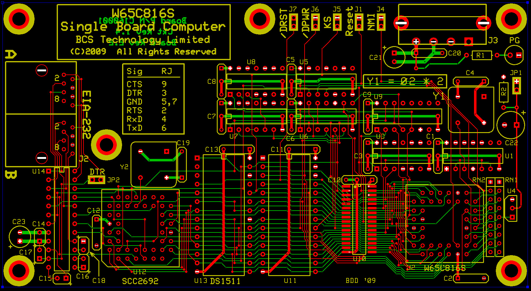
After several iterations of the design, I came up with a layout in which the SRAM was immediately to the left of the MPU (which is in a PLC44 socket), the EPROM to the left of the SRAM, the watchdog timer to the left of the EPROM and the DUART to the left of the watchdog. The reasoning behind this is the SRAM is connected A0-A15, the EPROM to A0-A12, the watchdog to A0-A4 and the DUART to A0-A3. This arrangement makes more sense when you also consider that all of the decoding logic is attached to the higher addresses, thus adding some length to those lines. To minimize the trace lengths to the decoding logic, I placed those ICs immediately above the MPU.
In all likelihood, I was overcautious with my layout, as PC motherboards seem to be able to get away with some pretty long traces to the PCI sockets, all of which operate at 33 MHz (much higher for PCI-X and PCI-E). I also used a four-layer board, both to improve noise and layer crosstalk immunity, and to not have to route individual power and ground traces everywhere.
POC V1.0 Printed Circuit Board
x86? We ain't got no x86. We don't NEED no stinking x86!
-
BigDumbDinosaur
- Posts: 9428
- Joined: 28 May 2009
- Location: Midwestern USA (JB Pritzker’s dystopia)
- Contact:
fachat wrote:
It seems that fixing the power supply on the CPU board has fixed my problem! Yesterday it ran for over an hour already, and it's been running for almost an hour now without issue.
x86? We ain't got no x86. We don't NEED no stinking x86!

BigDumbDinosaur wrote:
I also used a four-layer board, both to improve noise and layer crosstalk immunity, and to not have to route individual power and ground traces everywhere.
POC V1.0 Printed Circuit Board
POC V1.0 Printed Circuit Board
Can you share your reasoning for doing it this way as my education in this area is quite lacking. I must say you layed your board out very nicely and I can appreciate the time you took to optimize it.
Daryl
-
BigDumbDinosaur
- Posts: 9428
- Joined: 28 May 2009
- Location: Midwestern USA (JB Pritzker’s dystopia)
- Contact:
Bypassing
8BIT wrote:
I have a question for you concerning the bypass capacitors on your layout. I too have plans for a high-speed 65816-based system that would use the ExpressPCB 4-layer boards. In my design, I placed the caps like you did (near the Vcc pin), but I planned on having the caps legs connected directly to the respective power and ground layers. In your design, you bring the ground pin connection from the DIP IC's to the cap's using a thick surface trace. Also, you did the PLCC devices' caps directly to the power/ground planes.
Can you share your reasoning for doing it this way as my education in this area is quite lacking. I must say you layed your board out very nicely and I can appreciate the time you took to optimize it.
Daryl
Can you share your reasoning for doing it this way as my education in this area is quite lacking. I must say you layed your board out very nicely and I can appreciate the time you took to optimize it.
Daryl
As for the PLCC devices (MPU and DUART), I did directly connect each bypass cap to the associated device's Vcc pin. However, owing to the 100 mil grid layout used by the sockets, it wasn't practical to tie the device's ground pin to the bypass cap. This is not any particular disadvantage, due to the large area of the internal ground layer.
I have since determined from when I did the POC layout that the direct connection of the bypass cap to the device's ground terminal doesn't produce any significant improvement in noise suppression (based on 'scope observations). You will be okay in connecting your bypass caps directly to ground. However, I recommend the short and heavy direct connection between the device's Vcc pin and the bypass cap.
Incidentally, the bypass caps on my POC design are AVX SR275E104MAA multilayer ceramics, 0.1 mf at 50 volts. They are readily available from Mouser and others.
Also, I've developed a new board layout for POC 2.0, which includes an expansion port so I can test my yet-to-be-built SCSI host adapter. I'll put up a link to its picture when available.
x86? We ain't got no x86. We don't NEED no stinking x86!
-
BigDumbDinosaur
- Posts: 9428
- Joined: 28 May 2009
- Location: Midwestern USA (JB Pritzker’s dystopia)
- Contact:
Re: Bypassing
BigDumbDinosaur wrote:
Also, I've developed a new board layout for POC 2.0, which includes an expansion port so I can test my yet-to-be-built SCSI host adapter. I'll put up a link to its picture when available.
x86? We ain't got no x86. We don't NEED no stinking x86!