Now we've discussed a lot. But what problem are you actually trying to solve? For me it helps to explicitly list the requirements and design to purpose. Otherwise I tend to over-engineer if I don't watch out...
So what I read is (sorry if I missed something or over-interpret):
1. single-step the CPU - I guess from an external trigger (pushbutton or else)? single-stepping triggered by? released by? (after all, using an NMI and a timer, you can single-step the CPU just with software. I understand this is for debugging hardware and/or software, is it? It will be difficult to debug software as you need a specific hardware trigger. It is probably easier to use a logic analyzer circuit to trigger on specific hardware conditions (address, ...) to move into single-stepping mode. What is your intent?
2. hold the CPU for an undetermined amount of time, triggered by what? Similar question as 1. Released by what? pushbutton? What would that be for?
3. wait for slow peripherals - this again needs a hardware trigger, but can be derived from the select signal for such a slow device. However as the select signal keeps being active when the CPU is stopped (either with RDY or Phi2 stretched while high), a counter (even a single bit flipflops is a counter

) is required to disable the hold. As each device might need different delays, this is likely to be device-specific.
Are your devices capable of starting an access cycle in any of the CPU's cycle, or do they have their own (slower) clock, see below?
Anything I missed?
The only place I actually had to use RDY in my "classic" design was when I had a second CPU on the same bus. The second ("auxiliary") CPU was triggered by specific bus conditions (e.g. unmapped MMU page), and stopped the main CPU using RDY (while at the same time disabling RDY on the auxiliary CPU, so that it could start)
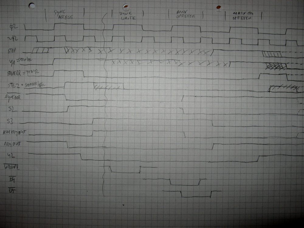
http://www.6502.org/users/andre/csa/auxcpu/index.html It could also be used to single-step/trace the main CPU, as one other bus condition was executing an opcode (SYNC) on a page where the MMU had a "no-execute" bit set. A screenshot from such a single step can be seen on my page.
This is actually a complex design. The timing diagram here
http://www.6502.org/users/andre/csa/auxcpu/timing1.jpg shows that I used a "2Phi2" clock to detect any relevant bus condition (either a switch from CPU to AUXCPU or back during phi2 high). Both CPUs are never on the bus at the same time, as you can see on the non-overlapping RDYOUT and AUXRDYOUT signals in the timing diagram (RDY is always released during phi2 low to give the main CPU time to react on it)
In my newer designs (with 65816 mostly) I use clock stretching when phi2 is high. It works by ORing the CPU's phi2 (and not necessarily I/O phi2, that can actually continue to run, depending on the device) with a stretch signal that is similar to RDY as generated above, but is not only set but also released during phi2 high.
Both those approaches work for devices that can start at any CPU clock cycle even if the access itself is slow. If you have a device with an own slow clock in the same clock domain, e.g. a 10MHz CPU, and a 1 MHz device where clocks are derived from the same source, you need to be able to detect the access at any of the 10 CPU cycles in the 1 MHz device cycle, and delay appropriately.
If you have CPU and devices in different clock domains (like a 10 MHz CPU clock derived from a 50MHz oscillator on an extension board, and 1 MHz I/O clock derived from a 16 MHz main board oscillator), it gets even more complicated and perhaps too much for that post.
So, long story short, what use cases do you have in mind? Can you list them and categorize them in the different situations I described? That should very much inform your circuitry.

