Why's this under programming? I'm not sure if I understand JML on the 65816. I think even in emulation mode it can be used to change the program bank register; if not then my memory map below falls apart.
I had a fairly normal 6502 style memory map going on. The first low 32KB mapped as RAM, the next 32KB mapped as ROM and devices sandwiched in at 00:7000. The great thing about that memory map is the reset vector can point to program code in the ROM space. Bog standard stuff. Then I allowed writes to RAM in ROM space and finally turned off ROM decoding making everything in bank zero RAM.
Now I'm wondering why?
If I (magically) have the reset vector pointing to 00FFF0 and magically make the 4 bytes starting at 00FFF0 encode the instruction
JML $24_bit_address then I effectively have reset vector than can be outside of bank 0.
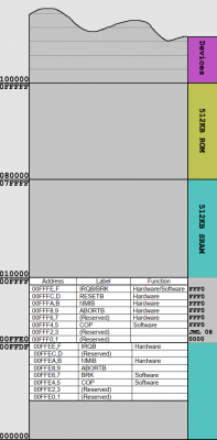
This opens up the following, pretty cool, memory map:
Attachment:
 Memory Map.png [ 91.46 KiB | Viewed 6646 times ]
That gives me 8 banks of RAM using a 512KB AS7C34096-8 SRAM and also 512KB of ROM using a SST39LF040-55 Flash. And makes address decoding a lot simpler.
Except for the 16 bytes jammed at the top of bank zero.
Be that as it may it can be decoded and those addresses can be sent off to a CPLD (like the ATF16V8) or even a diode ROM.
Just wondering if this is a complete brainfart or if it seems workable.
Cheers!
Andrew


