6502.org Forum  Projects  Code  Documents  Tools  Forum
It is currently Tue May 14, 2024 1:00 pm

All times are UTC


Post new topic Reply to topic  [ 164 posts ]  Go to page Previous  1 ... 5, 6, 7, 8, 9, 10, 11  Next
Author Message
PostPosted: Fri Sep 09, 2016 4:11 pm 
Offline
User avatar

Joined: Tue Jun 07, 2016 4:34 pm
Posts: 53
The ADSR registers bit:

Attachment:
ADSR_bit_IC.png
ADSR_bit_IC.png [ 15.96 KiB | Viewed 6500 times ]


Just two inverters with a clocked feedback loop:

Attachment:
ADSR_bit.png
ADSR_bit.png [ 18.1 KiB | Viewed 6500 times ]


The A, D and R values are gated so they are active only during the specific envelope phase:

Attachment:
adsr_gate_IC.png
adsr_gate_IC.png [ 84.22 KiB | Viewed 6500 times ]


The gates are controlled by the Gate bit and the R0 signal (counting direction):

Attachment:
adsr_gate.png
adsr_gate.png [ 11 KiB | Viewed 6500 times ]


So we have:

atk_gate = R0
dec_gate = ¬(rel_gate ∨ R0) = ¬R0 ∧ Gate
rel_gate = ¬(R0 ∨ Gate) = ¬R0 ∧ ¬Gate

One funny fact is that in the first cycle of the attack and decay phases the wrong rate is used, as the R0 line reacts with one cycle delay.


Top
 Profile  
Reply with quote  
PostPosted: Mon Sep 12, 2016 10:00 am 
Offline
User avatar

Joined: Fri Nov 09, 2012 5:54 pm
Posts: 1394
Finding out what happens in which PHI2 clock cycle inside the envelope generator
can be a bit tricky, and I think I would need to gain some "mental distance"
from the schematics for making a try. :)

While drfiemost was busy, I tried to dig into the rest of the SID,
and I think I should post my stuff before some of the details
start slipping from my memory...

;---

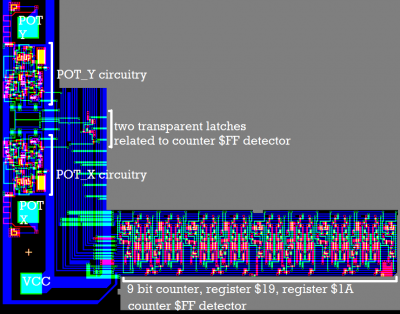
Now about the paddle related stuff:

Attachment:
paddle.png
paddle.png [ 128.57 KiB | Viewed 6451 times ]
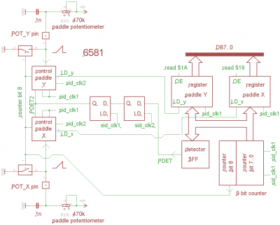

Block diagram:

Attachment:
paddle_block.png
paddle_block.png [ 23.85 KiB | Viewed 6451 times ]


We have a 9 bit counter running at PHI2 speed.

Bit 7..0 from the counter are fed into two 8 bit latches, POT_X and POT_Y.

At the POT_X pin, we have an external capacitor, which is charged
through the paddle potentiometer resistance to +5V.

When the voltage at the POT_X pin has reached a certain level,
the value from the counter is loaded into the POT_X register.

Also, when the coutner has reached $FF (maybe because the paddle
potentiometer is missing), there is some circuitry that forces
loading the counter value into POT_X.

It's a 9 bit counter, while the counter MSB ( bit 8 ) is 1,
the external capacitor is discharged through a FET in the SID
which is close to the POT_X pin.

Same thing for POT_Y.

;---

So one "conversion" from paddle potentiometer position to POT_X,POT_Y value
happens within every 512 PHI2 clock cycles.

Note, that PHI2 clock frequency is different for a PAL and a NTSC C64.

If the capacitors at the POT_X, POT_Y pins in both C64s would have
exactly the same value (usualy, they haven't),
...
and if the +5V supply voltages in both C64s would be exactly the same
(usually, it isn't),
...
reading out one and the same paddle position on both C64s
probably might give you a value that differs by 4% or such. :)


Top
 Profile  
Reply with quote  
PostPosted: Mon Sep 12, 2016 10:13 am 
Offline
User avatar

Joined: Fri Nov 09, 2012 5:54 pm
Posts: 1394
Now for the counter\register block.

Attachment:
paddle_cnt_latch.png
paddle_cnt_latch.png [ 69.77 KiB | Viewed 6449 times ]


;---

Even bits: low_active carry input, high_active carry output,
bit is stored in non_inverted form.

Attachment:
paddle_cnt_even.png
paddle_cnt_even.png [ 23.33 KiB | Viewed 6449 times ]


;---

Odd bits: high_active carry input, low_active carry output,
bit is stored in inverted form.

Attachment:
paddle_cnt_odd.png
paddle_cnt_odd.png [ 25.94 KiB | Viewed 6449 times ]


;---

The signal I had labeled 'PDET' is wired together for counter bit 7..0,
with a pullup to +5V. It is 1, when the counter is $FF.

//if one or more of the counter bits 7..0 is 0, PDET is tied to GND.

;---

The layout of the paddle counter looks completely different
from the layout of the envelope DAC counter...
but from the logic level design point of view,
the concept for both counters seems to be a little bit similar.

BTW:
To make the counter count, the low_active carry input of counter bit 0
is tied to GND. This connection is missing in the 6581 vectorized polygon
picture, but in the silicon it's there:

Attachment:
pad_cnt0_incarry.png
pad_cnt0_incarry.png [ 90.77 KiB | Viewed 6449 times ]


Edit: this connection only is missing in all the revisions of the 6581 polygon pictures.
In the 8580 polygon picture, the connection is there.


Last edited by ttlworks on Mon Sep 12, 2016 1:36 pm, edited 1 time in total.

Top
 Profile  
Reply with quote  
PostPosted: Mon Sep 12, 2016 10:21 am 
Offline
User avatar

Joined: Fri Nov 09, 2012 5:54 pm
Posts: 1394
Nothing fancy about the registers for POT_X, POT_Y.

Just another transparent latch loaded with LD_X (or LD_Y),
//don't know, why I had labeled them LD_$19 and LD_$1A in the picture.
with output enable and with a super buffer at the output
for driving the internal data bus.

Attachment:
paddle_register.png
paddle_register.png [ 11.73 KiB | Viewed 6449 times ]


It's a nice layout:
A big PolySi pad connected to a bit of the internal data bus,
then one bit of the POT_Y register east of the pad
and one bit of the POT_X register west of the pad.

Layout for the registers is the same...
just mirrored to make better use of the space on the silicon.


Top
 Profile  
Reply with quote  
PostPosted: Mon Sep 12, 2016 10:24 am 
Offline
User avatar

Joined: Fri Nov 09, 2012 5:54 pm
Posts: 1394
Then there are those two transparent latches between the register\counter block
and the circuitry close to the POT pins, delaying PDET by one clock cycle:

Attachment:
paddle_twoFFs.png
paddle_twoFFs.png [ 8.78 KiB | Viewed 6450 times ]


Top
 Profile  
Reply with quote  
PostPosted: Mon Sep 12, 2016 10:30 am 
Offline
User avatar

Joined: Fri Nov 09, 2012 5:54 pm
Posts: 1394
Now the circuitry close to the POT_X pin.
//POT_Y seems to have an identical layout, just mirrored.

Attachment:
paddle_logic.png
paddle_logic.png [ 71.86 KiB | Viewed 6449 times ]


Schematic:

Attachment:
paddle_control.png
paddle_control.png [ 192.68 KiB | Viewed 6449 times ]


Those two FETs working as a voltage comparator during sid_clk1 =1
and as a R\S flipflop with logic level outputs during sid_clk2 =1
gave me quite a headache.

So much for the paddles.

;---

Edit: July 2023:
It appears that there is an error in my schematic:

Attachment:
paddle_control_err.png
paddle_control_err.png [ 117.83 KiB | Viewed 4593 times ]


Last edited by ttlworks on Fri Jul 28, 2023 7:02 am, edited 1 time in total.

Top
 Profile  
Reply with quote  
PostPosted: Mon Sep 12, 2016 11:20 am 
Offline
User avatar

Joined: Fri Nov 09, 2012 5:54 pm
Posts: 1394
The 8580 clock generator is completely different from the 6581 clock generator.

I'm now posting my interpretation of it...
But if you want to be on the safe side, you better consult an engineer. :)

Attachment:
8580_clk.png
8580_clk.png [ 165.23 KiB | Viewed 6440 times ]


Anyhow, for simulating a SID or for building your own SID with TTL parts
it isn't neccessary to understand the clock generator.

;---

BTW: in the vectorized 8580 polygon picture, it appears that some part
on the diffusion layer was missing. In the silicon, it seems to be there...
it's just very hard to spot:

Attachment:
8580_clk1_diff.png
8580_clk1_diff.png [ 4.95 KiB | Viewed 6440 times ]


;===

Edit: Message from drfiemost about the 8580 clock generator:

Attachment:
Phi2_pin_8580.png
Phi2_pin_8580.png [ 59.19 KiB | Viewed 6388 times ]


Althought arranged differently it looks like yours. I had verified it through the perfect6502 emulator, the only problem is that I had to short
the big capacitors and open the small ones as the analogic components are not supported. I hope this won't affect the validity of the result.


Last edited by ttlworks on Wed Sep 14, 2016 6:01 am, edited 1 time in total.

Top
 Profile  
Reply with quote  
PostPosted: Mon Sep 12, 2016 11:23 am 
Offline
User avatar

Joined: Thu Dec 11, 2008 1:28 pm
Posts: 10800
Location: England
ttlworks wrote:
BTW: in the vectorized 8580 polygon picture, it appears that some part
on the diffusion layer was missing. In the silicon, it seems to be there...
it's just very hard to spot

Lots of good work in these posts, thanks. A great advantage the visual6502 effort had was building and running the simulation in parallel with doing the vectorising. The simulation found a few bugs in the polygons. I'm sure there were also pure simulation bugs to be found too!


Top
 Profile  
Reply with quote  
PostPosted: Mon Sep 12, 2016 12:01 pm 
Offline
User avatar

Joined: Fri Nov 09, 2012 5:54 pm
Posts: 1394
Thanks for the kind words, BigEd.

While dissecting the polygon images, we found two more bugs:

;---

In the 8580, a part on the diffusion layer of the noise LFSR clock generator seems to be missing.
(all three channels)
Attachment:
8580_noiseclk_diff.png
8580_noiseclk_diff.png [ 180.33 KiB | Viewed 6435 times ]


;---

In _all_ of the 6581 revisions, a via in the write signal for the upper PWM registers is missing.
(all three channels)
Attachment:
6581_pwmreg_diff.png
6581_pwmreg_diff.png [ 12.67 KiB | Viewed 6438 times ]


;---

At some point, me and drfiemost had started to wonder how much time and effort
went into generating those vectorized polygon pictures.

It's a manually routed chip layout, silicon might have some impurities,
so automated tools for processing the silicon picture probably won't bring you far.

Just trying to figure out what the diffusion layer might look like for one of the
sprite X\Y registers in a VIC2 took me a full day. :)
Considering this, only having four bugs in the polygon pictures of the SID
is very impressive !

;---

With our little SID dissection here in the forum, we are standing on the shoulders
of those who de_capped the chips, made the high resolution silicon pictures,
and generated the vectorized polygon pictures.


Without this work being done before, we would have had as much chance as a snowball in hell...


Last edited by ttlworks on Mon Sep 12, 2016 12:15 pm, edited 2 times in total.

Top
 Profile  
Reply with quote  
PostPosted: Mon Sep 12, 2016 12:05 pm 
Offline
User avatar

Joined: Thu Dec 11, 2008 1:28 pm
Posts: 10800
Location: England
What's wrong with the diffusion? Or is that image a 'repaired' image? Could you post a crop of the silicon for that area?


Top
 Profile  
Reply with quote  
PostPosted: Mon Sep 12, 2016 12:27 pm 
Offline
User avatar

Joined: Thu Dec 11, 2008 1:28 pm
Posts: 10800
Location: England
(I've posted about the general problem of polygon capture over here.)


Top
 Profile  
Reply with quote  
PostPosted: Mon Sep 12, 2016 12:28 pm 
Offline
User avatar

Joined: Fri Nov 09, 2012 5:54 pm
Posts: 1394
Quote:
What's wrong with the diffusion?

The output of the NOR gate is unconnected, but I think it should be connected to the PolySi trace above.
It was drfiemost who had spotted this bug, and I can't remember exactly...
Attachment:
8580_noiseclk_diff1.png
8580_noiseclk_diff1.png [ 138.79 KiB | Viewed 6432 times ]


Top
 Profile  
Reply with quote  
PostPosted: Mon Sep 12, 2016 12:35 pm 
Offline
User avatar

Joined: Thu Dec 11, 2008 1:28 pm
Posts: 10800
Location: England
Goodness me, those edges are incredibly faint! But you must be right - the NOR output should go somewhere. (Unless it isn't needed.) Again, I think in the pre-simulation phase some of the bugs found are things like a logic input which is not driven by anything, which is a strong indication of a problem, or as in this case, a logic output not driving anything, which is a likely indication of a problem.


Top
 Profile  
Reply with quote  
PostPosted: Mon Sep 12, 2016 12:54 pm 
Offline
User avatar

Joined: Fri Nov 09, 2012 5:54 pm
Posts: 1394
In the 6581, the output of the NOR _is_ connected to that trace.
The layout is different from the 8580 silicon, of course.
Attachment:
8580_noiseclk_diff2.png
8580_noiseclk_diff2.png [ 9.77 KiB | Viewed 6424 times ]


What worries me a bit is, that it's a 'systematical error',
means for each one of the three oscillator channels the connection is missing.

It's a nice thing, that the bugs are different for the 6581 and the 8580 polygon pictures,
so one could compare the pictures from both chips when the circuitry of interest is supposed
to do the same in both chips. :)


Top
 Profile  
Reply with quote  
PostPosted: Mon Sep 12, 2016 1:00 pm 
Offline
User avatar

Joined: Thu Dec 11, 2008 1:28 pm
Posts: 10800
Location: England
We do tend to see what we expect to see - which helps a lot in making sense of these very faint ambiguous images. But sometimes it leads us astray! You are getting a benefit from having two people working at the same time in cooperation.


Top
 Profile  
Reply with quote  
Display posts from previous:  Sort by  
Post new topic Reply to topic  [ 164 posts ]  Go to page Previous  1 ... 5, 6, 7, 8, 9, 10, 11  Next

All times are UTC


Who is online

Users browsing this forum: No registered users and 3 guests


You cannot post new topics in this forum
You cannot reply to topics in this forum
You cannot edit your posts in this forum
You cannot delete your posts in this forum
You cannot post attachments in this forum

Search for:
Jump to:  
cron