6502.org Forum  Projects  Code  Documents  Tools  Forum
It is currently Thu Nov 21, 2024 8:36 pm

All times are UTC


Post new topic Reply to topic  [ 213 posts ]  Go to page Previous  1 ... 7, 8, 9, 10, 11, 12, 13 ... 15  Next
Author Message
 Post subject: Re: Breaking 6502 apart
PostPosted: Fri Jan 25, 2013 9:38 pm 
Offline
User avatar

Joined: Fri Jun 22, 2012 7:39 am
Posts: 201
Hello my friends! And happy new year)

I continued my investigation of 6502 CPU and started to stream it live daily (on russian :D ) :
http://www.youtube.com/watch?v=--etCODbhto

(you can see other videos on my youtube channel : http://www.youtube.com/user/Andorianin )

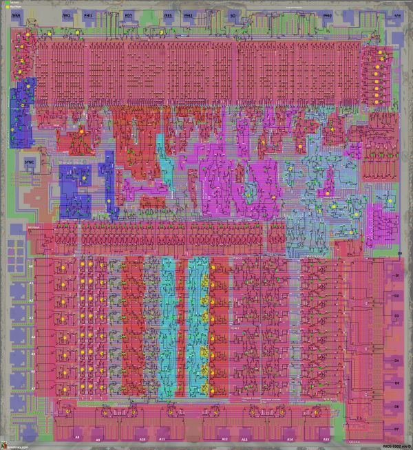
As result I improved 6502 circuit and studied meaning of some random logic parts :
Image

Purple areas : branch / flow
Red areas : ALU
Blue areas : interrupt-related processing
Cyan : BCD-correction related things
And bright areas are flags (except small blue area on top-right corner near PLA 96 line). Other areas with same bright-red color are just separated between each other.

Updated PSD here : http://breaknes.com/files/6502/6502.zip (140 MB)

_________________
6502 addict


Top
 Profile  
Reply with quote  
 Post subject: Re: Breaking 6502 apart
PostPosted: Sun Jan 27, 2013 3:21 pm 
Offline
User avatar

Joined: Thu Dec 11, 2008 1:28 pm
Posts: 10985
Location: England
Nice! I don't quite see which areas you mean with "same bright-red color"
I think the dull light blue at middle right is the area you mean to highlight as holding the 6 bits of the status register.
I didn't quite understand what you mean by 'bright areas' - do you mean more than these 6?


Top
 Profile  
Reply with quote  
 Post subject: Re: Breaking 6502 apart
PostPosted: Sun Jan 27, 2013 5:58 pm 
Offline
User avatar

Joined: Fri Jun 22, 2012 7:39 am
Posts: 201
For example instruction register or secondary cycle counter (T2-T5) are the "same bright-red color" areas)
"Bright areas" are 6 bits of status register + its set/clear logic.

_________________
6502 addict


Top
 Profile  
Reply with quote  
 Post subject: Re: Breaking 6502 apart
PostPosted: Sun Jan 27, 2013 6:20 pm 
Offline
User avatar

Joined: Thu Dec 11, 2008 1:28 pm
Posts: 10985
Location: England
Ah, I see. By 'bright' you mean 'less saturated' perhaps? The red looks faded. But I see the area you mean now.
Cheers
Ed


Top
 Profile  
Reply with quote  
 Post subject: Re: Breaking 6502 apart
PostPosted: Fri Feb 01, 2013 9:57 pm 
Offline
User avatar

Joined: Fri Jun 22, 2012 7:39 am
Posts: 201
Hello, today I finally completed ALU.

I wrote some documentation on it, and made some tests for decimal mode. You can find it below.

ALU internals

ALU Inputs:

I/ADDC : input carry (inverted)
/DAA, /DSA : used for decimal correction:
for ADC /DAA=0,/DSA=1; for SBC /DAA=1,/DSA=0.
/DSA = /DAA = 1, when D flag cleared.

3 sorts of command lines: input controls, operation controls, output controls.
+ 2 input registers : AI (A input) and BI (B input)

Input controls:
0/ADD : 0 -> AI
SB/ADD : special bus -> AI
DB/ADD : data bus -> BI
nDB/ADD : inverted data bus -> BI
ADL/ADD : ADL -> BI
SB/AC : special bus (+ decimal correction) -> accumulator

Operation controls:
ORS : A | B
ANDS: A & B
EORS: A ^ B
SUMS: A + B + carry
SRS : shift right to 1

Output controls:
- from adder hold register:
ADD/SB06 : adder hold[0-6] -> SB[0-6]
ADD/SB7 : adder hold[7] -> SB[7]
ADD/ADL : adder hold -> ADL
- from accumulator:
AC/SB : accumulator -> special bus
AC/DB : accumulator -> data bus
SB/DB : special bus = data bus

Internal registers:
ADD : adder hold register for intermediate result (before decimal correction).
Also can be used for address calculation.
AC : accumulator. Hold final add/subtract result, after optional decimal correction.

Random notes and facts:

- ALU has inverted carry chain between odd/even bits, to reduce propagation delay.
- ALU write intermediate result to adder hold register (ADD) during PHI2, and updating accumulator (AC) at same time.
Final result placed on acumulator only on following PHI1 half-cycle.
This is need to make sure no conflicts happen, during refreshing of AC register.
To ensure this, AC-loading control lines are grounded during PHI2.
- a + b + carry is actually a ^ b ^ carry.
- Decimal correction is actually +6

To add A + B, do the following:
- put A on special bus (SB)
- put B on data bus (DB)
- optionally set input carry
- wait dummy PHI1 half-cycle
- if you need to add in decimal mode, set /DAA = 0, /DSA = 1.
- perform commands on next PHI2 : SB/ADD, DB/ADD, SUMS
- perform commands on next PHI1 : ADD/SB06, ADD/SB7, SB/AC
- get result from accumulator (AC)

To subtract A - B, do the following:
- put A on special bus (SB)
- put B on data bus (DB)
- force to set input carry
- wait dummy PHI1 half-cycle
- if you need to subtract in decimal mode, set /DAA = 1, /DSA = 0.
- perform commands on next PHI2 : SB/ADD, NDB/ADD (<-- DB is loaded as inverted value), SUMS
- perform commands on next PHI1 : ADD/SB06, ADD/SB7, SB/AC
- get result from accumulator (AC)

So basically A - B = A + NOT(B) + 1

ALU pipeline :
- load input registers (AI and BI)
- ORS, ANDS, SRS: perform logic operations, based on NAND and NOR
- EORS: perform exclusive-OR, based on NAND/NOR
- SUMS: calculate sum of two operands based on XOR and additional XOR it with carry
- DAA: calculate decimal carry and half-carry on-the-fly
- hold intermediate result in ADD register
- set output carry and overflow flags
- output carry is set whenever binary carry or decimal carry happens
- DSA: perform decimal adjustment (+6) to intermediate result and put it on accumulator

ALU circuit

Image

Nicely cleaned and correct.

ALU Simulation

You can find it on Google code : http://code.google.com/p/breaks/source/ ... 6502/ALU.c

Decimal mode tests

ALU tests in decimal mode, based on :
http://visual6502.org/wiki/index.php?ti ... ecimalMode

ADC: AI + BI + Carry = AC, V out, C out

79 + 00 + 1 = 80, V:1, C:0
24 + 56 + 0 = 80, V:1, C:0
93 + 82 + 0 = 75, V:1, C:1
89 + 76 + 0 = 65, V:0, C:1 !!! result!
89 + 76 + 1 = 66, V:0, C:1 !!! result!
80 + F0 + 0 = D0, V:1, C:1
80 + FA + 0 = E0, V:1, C:1 !!! V-flag
2F + 4F + 0 = 74, V:0, C:0
6F + 00 + 1 = 76, V:0, C:0

SBC: AI + !BI + Carry = AC, V out, C out

00 - 00 + 0 = 99, V:0, C:0
00 - 00 + 1 = 00, V:0, C:1
00 - 01 + 1 = 99, V:0, C:0
0A - 00 + 1 = 0A, V:0, C:1
0B - 00 + 0 = 0A, V:0, C:1
9A - 00 + 1 = 9A, V:1, C:1 !!! V-flag
9B - 00 + 0 = 9A, V:1, C:1 !!! V-flag

By !!! I marked some differencies. Looks like Visual6502 has some problems in decimal mode. Because if you look, for example on 89 + 76, it should be 0x165 (0x65 + carry), but Visual6502 somehow has 0x55 as a result, which is incorrect of couse.

Additional reading

US Patent 3991307 : http://www.google.com/patents/US3991307

Its really nothing to say anything else, its done :mrgreen:

_________________
6502 addict


Top
 Profile  
Reply with quote  
 Post subject: Re: Breaking 6502 apart
PostPosted: Sun Feb 03, 2013 10:04 am 
Offline
User avatar

Joined: Thu Dec 11, 2008 1:28 pm
Posts: 10985
Location: England
I'd be surprised if visual6502 had any problems in decimal mode! For the 89+76+0 example, I ran
http://www.visual6502.org/JSSim/expert. ... a&steps=20
and got the expected result $65, V clear and C set.

Please could you elaborate?

Thanks
Ed


Top
 Profile  
Reply with quote  
 Post subject: Re: Breaking 6502 apart
PostPosted: Sun Feb 03, 2013 4:08 pm 
Offline
User avatar

Joined: Fri Jun 22, 2012 7:39 am
Posts: 201
Possible this link :
http://visual6502.org/wiki/index.php?ti ... ecimalMode

has typo here:

Tests for ADC
89 + 76 and C=0 gives 55 and N=0 V=0 Z=0 C=1 (simulate)

And nothing else)

_________________
6502 addict


Top
 Profile  
Reply with quote  
 Post subject: Re: Breaking 6502 apart
PostPosted: Sun Feb 03, 2013 4:30 pm 
Offline
User avatar

Joined: Thu Dec 11, 2008 1:28 pm
Posts: 10985
Location: England
ah, yes, typos in that table could be the problem. I'll investigate.


Top
 Profile  
Reply with quote  
 Post subject: Re: Breaking 6502 apart
PostPosted: Sun Feb 10, 2013 4:05 pm 
Offline
User avatar

Joined: Fri Jun 22, 2012 7:39 am
Posts: 201
I found meaning of some internal control lines, especially T5 and T6 cycles, for extra-long instructions, like BRK and some shift/rotate, which takes 7 cycles (T0...T6).
Last extra cycle (T6) has no output to decoder, but disributed internally, through T6 control line. Its simply 1-cycle delayed T5.
Instruction decoder activate processing of such long instructions by "TX" lines, where X mean "dont care which cycle is it".

I updated circuit (see above for JPG image)

Updated PSD here : http://breaknes.com/files/6502/6502.zip (141 MB)

Now random logic looks trivial to me :) I decided to understand how its actually work, instead of blind NAND/NOR simulation.

_________________
6502 addict


Top
 Profile  
Reply with quote  
 Post subject: Re: Breaking 6502 apart
PostPosted: Mon Feb 25, 2013 6:48 pm 
Offline
User avatar

Joined: Fri Jun 22, 2012 7:39 am
Posts: 201
Started to implement 6502 in DRAGON:


Attachments:
6502_diag.png
6502_diag.png [ 76.84 KiB | Viewed 3588 times ]

_________________
6502 addict
Top
 Profile  
Reply with quote  
 Post subject: Re: Breaking 6502 apart
PostPosted: Mon Feb 25, 2013 7:28 pm 
Offline
User avatar

Joined: Thu Dec 11, 2008 1:28 pm
Posts: 10985
Location: England
Hmm - is that http://en.wikipedia.org/wiki/DRAKON ?
Cheers
Ed


Top
 Profile  
Reply with quote  
 Post subject: Re: Breaking 6502 apart
PostPosted: Tue Feb 26, 2013 5:13 am 
Offline
User avatar

Joined: Fri Jun 22, 2012 7:39 am
Posts: 201
Yeah, this one.
I'm using http://drakon-editor.sourceforge.net/ for flowcharts and generate C, as output.
You can get latest drakon-chart on SVN: /breaks/Breaks6502/drakon/

_________________
6502 addict


Top
 Profile  
Reply with quote  
 Post subject: Re: Breaking 6502 apart
PostPosted: Tue Feb 26, 2013 1:43 pm 
Offline
User avatar

Joined: Fri Jun 22, 2012 7:39 am
Posts: 201
Top part ready :D


Attachments:
6502_diag.png
6502_diag.png [ 129.18 KiB | Viewed 3557 times ]

_________________
6502 addict
Top
 Profile  
Reply with quote  
 Post subject: Re: Breaking 6502 apart
PostPosted: Mon Mar 11, 2013 12:18 pm 
Offline
User avatar

Joined: Fri Jun 22, 2012 7:39 am
Posts: 201
Polished circuit again and fixed small errors :
Image

_________________
6502 addict


Top
 Profile  
Reply with quote  
 Post subject: Re: Breaking 6502 apart
PostPosted: Mon Mar 11, 2013 12:28 pm 
Offline
User avatar

Joined: Thu Dec 11, 2008 1:28 pm
Posts: 10985
Location: England
Very nice! What's the state of play with the simulation? Have you reached the difficulty of the bidirectional pass gates in the datapath yet?
Cheers
Ed


Top
 Profile  
Reply with quote  
Display posts from previous:  Sort by  
Post new topic Reply to topic  [ 213 posts ]  Go to page Previous  1 ... 7, 8, 9, 10, 11, 12, 13 ... 15  Next

All times are UTC


Who is online

Users browsing this forum: No registered users and 5 guests


You cannot post new topics in this forum
You cannot reply to topics in this forum
You cannot edit your posts in this forum
You cannot delete your posts in this forum
You cannot post attachments in this forum

Search for:
Jump to: