6502.org Forum  Projects  Code  Documents  Tools  Forum
It is currently Mon May 20, 2024 2:13 pm

All times are UTC


Post new topic Reply to topic  [ 37 posts ]  Go to page Previous  1, 2, 3  Next
Author Message
PostPosted: Mon Aug 28, 2023 11:45 pm 
Offline

Joined: Fri Mar 18, 2022 6:33 pm
Posts: 449
This is really cool. I like how you're taking things a different direction from a lot of hobby projects, particularly with that LED panel for output, and manual entry for input.

_________________
"The key is not to let the hardware sense any fear." - Radical Brad


Top
 Profile  
Reply with quote  
PostPosted: Mon Aug 28, 2023 11:58 pm 
Offline
User avatar

Joined: Wed May 31, 2023 10:46 pm
Posts: 26
Location: Sebastopol, California
Paganini wrote:
This is really cool. I like how you're taking things a different direction from a lot of hobby projects, particularly with that LED panel for output, and manual entry for input.


The alternate design choices I think come from the combination of doing a fairly extreme version of bootstrapping (no built computers or programs etc) and trying to simplify the design while still getting to keyboard+display+assembler+storage. I almost went with bare-bones NTSC, but this was even easier, and for me a new thing (I had done bit banging NTSC decades ago).

If you or anyone can point me to existing art on interleaving video and CPU access to an SRAM at high clock speeds, that would be great!

_________________
--Mark


Top
 Profile  
Reply with quote  
PostPosted: Tue Aug 29, 2023 4:39 am 
Offline

Joined: Mon Jan 19, 2004 12:49 pm
Posts: 691
Location: Potsdam, DE
A couple of unexpected pixels: the first few leftmost of the red block, and the bottom right pixel. Are they the ones you mentioned as damaged?


Top
 Profile  
Reply with quote  
PostPosted: Tue Aug 29, 2023 7:38 am 
Offline
User avatar

Joined: Wed May 31, 2023 10:46 pm
Posts: 26
Location: Sebastopol, California
barnacle wrote:
A couple of unexpected pixels: the first few leftmost of the red block, and the bottom right pixel. Are they the ones you mentioned as damaged?

Yes, the upper left side as pictured is where a fair number of SMD pixels got knocked off before I got the module, the the lower right is where the SMD pixel is still there but is kind of half on (if I press it down just right the green and blue light up). I've ordered a couple more modules of the same type...crossing my fingers at least one will be intact!

_________________
--Mark


Top
 Profile  
Reply with quote  
PostPosted: Tue Aug 29, 2023 11:42 am 
Offline

Joined: Fri Jul 09, 2021 10:12 pm
Posts: 741
SpiradiscGuy wrote:
If you or anyone can point me to existing art on interleaving video and CPU access to an SRAM at high clock speeds, that would be great!

I've built several different 6502 systems like that. I think my main advice is not to interleave access to the CPU's main memory in the fashion of old 8-bit computers, especially if you need higher clock speeds - it is better to have a separate pool of video memory with its own buses, and only let the CPU access it when it really needs to.

Better still, only provide write access to that memory - this relaxes the timing constraints and allows a less synchronous design. RAM is cheap these days and your resolution is low enough that if you do need read access, you can easily maintain a shadow copy in your system RAM and read back from that when needed. It is still simplest if the CPU clock is the same as the video system's memory clock, but that's no longer essential with a write-only interface.

For the video memory, your video circuit is going to access its memory at a certain steady rate - e.g. for VGA I used 6.3MHz. This bus cycle period is then divided into four stages. In stage 0 the video circuit drives counter outputs onto the address bus. In stage 1 the video circuit reads and latches data from video RAM so that it can continue to output that data to the screen and no longer needs the buses during stages 2 and 3. Then if there's a pending write from the CPU, then in stage 2 the appropriate address is driven to the video address bus and in stage 3 the write enable takes place.

Zooming out a bit, during stages 0 and 1 the video circuit owns the video buses, and in stages 2 and 3, the CPU does if it wants to. If you are running this in sync with the CPU clock then you want the CPU clock to be high during stages 2 and 3.

The main other thing you need is a way to multiplex the video address and data buses, so that they can be driven either by the video circuit or by the CPU. You can use multiplexers of course, or you can use bus transceivers and/or tristate counters. I've always preferred the latter approach - I put bus transceivers between the CPU buses and the video bus, and use tristate counters for address generation within the video circuit so I don't need more transceivers between them and the video bus. Then the counter outputs are enabled for stages 0 and 1, and during stages 2 and 3 the CPU-side bus transceivers are enabled.

You may need a bit more control over the exact timing of the various signal changes that take place during the bus cycle, so it can be helpful to have a faster clock with e.g. 8 ticks per bus cycle. I've mostly got away with only 4 ticks, and sometimes used gate delays to shift things a bit, but that wasn't the most reliable of approaches.

As you can tell, I could write about this all day, but I don't want to detract from the experience of figuring it out yourself! But do ask if there's anything you want to discuss.

Here are two of my past projects for reference - the first is a standard-definition TV based system, which does share main system memory with the video circuit, but only needs to run at quite slow frequencies. Page 6 of the schematic covers the memory subsystem. https://github.com/gfoot/compvideo6502

The second is more recent, for VGA resolutions: https://github.com/gfoot/simplevga6502 This branch on github outputs 160x100, and there are other branches for higher resolutions but the circuits get more complex so this is the best one for quick reference on the bus architecture, which didn't change much in later revisions. This design has separate video memory, with write-only access from the CPU as I advised above. At the point of upgrading to 800x600 I regretted how closely-tied the CPU frequency was to the video frequency, as it made it very hard to diagnose stability issues, and next time around I'm going to decouple that for sure.


Top
 Profile  
Reply with quote  
PostPosted: Tue Aug 29, 2023 2:09 pm 
Offline
User avatar

Joined: Mon Aug 30, 2021 11:52 am
Posts: 269
Location: South Africa
gfoot wrote:
The second is more recent, for VGA resolutions: https://github.com/gfoot/simplevga6502 This branch on github outputs 160x100, and there are other branches for higher resolutions but the circuits get more complex so this is the best one for quick reference on the bus architecture, which didn't change much in later revisions.
A quick question (and I'm hopefully I'm not derailing the thread too much). Simple VGA runs a resolution of 160x100 and looks like it has 16KB of addressable memory. However it's using a 640x400 screen resolution. Pixel doubling / quadrupling in the horizontal can be done by presenting the same colour 2 or 4 times to the VGA DAC before moving onto the next pixel. But how do you achieve vertical quadrupling? Do you redraw the same row 4 times? I haven't solved this yet and just assumed I've have to re-latch the address counter back to what it was at the start of the row three times, and then allow it to continue counting to the next address at the end of the fourth row. Or is enough to just divide all the vertical signal times by 4 and let the monitor sort it out?

gfoot wrote:
This design has separate video memory, with write-only access from the CPU as I advised above. At the point of upgrading to 800x600 I regretted how closely-tied the CPU frequency was to the video frequency, as it made it very hard to diagnose stability issues, and next time around I'm going to decouple that for sure.
A design I've doodled on paper but only partially tested is to use 74HCT40105 4bit FIFOs. Put 8bits of data in two of the '40105s and put 16bits of address in another four '40105s. Then tick data out of all the '40105s at a constant 20MHz (assuming horizontally pixel doubled 800x600). This allows the video data to be read out when the video clock is low and written in when the clock is high (or vice-versa).


Top
 Profile  
Reply with quote  
PostPosted: Tue Aug 29, 2023 4:20 pm 
Offline

Joined: Fri Jul 09, 2021 10:12 pm
Posts: 741
I don't want to derail Mark's thread too much - but:

AndrewP wrote:
But how do you achieve vertical quadrupling? Do you redraw the same row 4 times?

Yes. Using separate counters for horizontal and vertical coordinates means that you can just not wire the low bits through to the memory, to double, quadrupole, etc the scanlines.

Quote:
A design I've doodled on paper but only partially tested is to use 74HCT40105 4bit FIFOs. Put 8bits of data in two of the '40105s and put 16bits of address in another four '40105s. Then tick data out of all the '40105s at a constant 20MHz (assuming horizontally pixel doubled 800x600). This allows the video data to be read out when the video clock is low and written in when the clock is high (or vice-versa).

That's interesting. My best plan was to use counters so that they could automatically increment, but I haven't really thought it through, there are a lot of options.


Top
 Profile  
Reply with quote  
PostPosted: Tue Aug 29, 2023 5:04 pm 
Offline

Joined: Fri Mar 18, 2022 6:33 pm
Posts: 449
SpiradiscGuy wrote:
If you or anyone can point me to existing art on interleaving video and CPU access to an SRAM at high clock speeds, that would be great!
Others here are a lot more versed in this than I am - I went with dual-port RAM for my VGA circuit. However, "The CRT Controller Handbook" by Gerry Kane is an excellent resource and has a brief discussion of multiplexing the bus for interleaved access. You might also check out some old data sheets, such as the one for the Hitachi HD6845SP. I also have a book called "Using Microprocessors and Microcomputers: The 6800 Family" by Greenfield and Wray that has an entire appendix devoted to implementing a video terminal. In general, any of the old CRT controller documentation will touch on this subject. Also, I think Chad (forum member sburrow) did this successfully with his Acolyte board. IIRC, he simply fed Ø2 into the bus enable pin of the 6502 to disconnected it every half cycle!

_________________
"The key is not to let the hardware sense any fear." - Radical Brad


Top
 Profile  
Reply with quote  
PostPosted: Tue Aug 29, 2023 5:28 pm 
Offline

Joined: Fri Dec 21, 2018 1:05 am
Posts: 1076
Location: Albuquerque NM USA
I have an Apple II style graphic design where W65C02 shares video RAM at different phase of the clock. I was able to achieve 12.6Mhz for 6502 cpu clock, half the VGA clock. Unfortunately I use CPLD for logic which is fast, but not consistent with your locked room requirements.
viewtopic.php?f=4&t=6955


Top
 Profile  
Reply with quote  
PostPosted: Tue Aug 29, 2023 8:43 pm 
Offline
User avatar

Joined: Fri Aug 03, 2018 8:52 am
Posts: 746
Location: Germany
AndrewP wrote:
But how do you achieve vertical quadrupling? Do you redraw the same row 4 times? I haven't solved this yet and just assumed I've have to re-latch the address counter back to what it was at the start of the row three times, and then allow it to continue counting to the next address at the end of the fourth row. Or is enough to just divide all the vertical signal times by 4 and let the monitor sort it out?

i can tell you how i've done it with my current VGA card:
I take the values of the X and Y counters used for the sync signals to calculate the address to read data from.
you're just converting a 2D index into a 1D one, so the math is simple to do in hardware: ((Y * bytes_per_row) + X) + base_address. except not the full width of the Y counter is used. depending on how many lines you want to duplicate you cut off the bottom n bits (basically shifting Y to the right by n bits) before using it for the math. that way the repeating accesses just come naturally.
the left over bits are then used to decide when the final scanline is being drawn to allow the memory access to "escape the loop".
what i mean is that when you're drawing the n'th pixel you're accessing memory for the n+1'th pixel. so when you're at the end of the current scanline the video circuit has to decide if it should load the first pixel of the next scanline, or the first pixel of the current one (which is what you want for drawing the same scanline multiple times in a row).
so that's what the bottom n bits are used for, when all of them are 1, the video circuit is at the last duplicated scanline and is therefore allowed to read the first pixel of the next line at the end of the current one.

i hope that was somewhat understandable, i could show you a screenshot of the circuit i use in my CPLD, but honestly i think that's even less useful
Attachment:
javaw_BGWgPiqIdb.png
javaw_BGWgPiqIdb.png [ 471.4 KiB | Viewed 4403 times ]

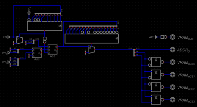
i'm only duplicating a line twice for 320x200, so PY1 refers to the bottom bit of PY (Pixel Y Counter) while PY8 are bits 1-8 of PY, the AND gate on the upper left corner is used for the scanline access wrapping, and the other larger AND gate is for frame wrapping (so the last access loads the first pixel of the next frame).

AndrewP wrote:
A design I've doodled on paper but only partially tested is to use 74HCT40105 4bit FIFOs. Put 8bits of data in two of the '40105s and put 16bits of address in another four '40105s. Then tick data out of all the '40105s at a constant 20MHz (assuming horizontally pixel doubled 800x600). This allows the video data to be read out when the video clock is low and written in when the clock is high (or vice-versa).

FIFOs are pretty useful when it comes to video as you can have different rates for loading bytes and pushing stuff to the screen. for example if cycle interleaving with the CPU is too difficult to pull off, you could probably just pause the CPU every now and then, burst load a bunch of bytes into the FIFO, and then unpause the CPU again.
if you're using a IDT720x or similar FIFO with a "Half Full" output you could have the burst happen automatically when the FIFO is only half filled, to then top it off.

that also reminds me of a concept i made for a fully software controlled VGA controller. ie a seperate 65C02 running at 20-25MHz that manually loads some IDT720x FIFOs with data which is then used by a VGA circuit to draw pixels on a screen.
more specifically there would be 1 FIFO for each duplicated scanline which are all wired together on the CPU side so all of them get loaded with the same data in parallel. then on the Video output side the first scanline uses the first FIFO, second scanline uses the second FIFO, etc. that way the CPU doesn't have to load the same data multiple times in a row.
for example (using 640x480 as a base), for 320x240 (or 320x200) you need 2 parallel FIFOs. for 160x120 (or 160x100) you would need 4.

main question is, can the CPU keep up with the video bandwidth? for 320x200 @ 4bpp (bits per pixel) a whole line of pixels is 160 Bytes and (assuming the CPU runs at 25MHz) you'd had 1600 clock cycles (800 cycles per full scanline) to load those into the FIFO (or 10 cycles per byte). but there is also the vertical blanking period, which helps.
so averaging this out to a whole frame you need to load 32000 Bytes within 420000 Cycles which is 13.125 Cycles per Byte, not much better and would require a tight copying loop.
160x100 @ 4bpp is a lot more feasible but the resolution is also very... economical. running the CPU at 12.5MHz (which is also easier to achieve) you get 210000 Cycles per frame to load 8000 Bytes, which comes out to 26.25 Cycles per Byte.
of course if you use a higher bit depth, like 8 bpp, then you're back on 13.125 Cycles per Byte as you need to load twice the amount of data per frame.

then again, at those resolutions it seems WAY easier to just get some cheap 8kB Dual Port RAM ICs and have the CPU and Video side seperate and doing their own thing. (16kB is also an option but it's twice the price, i have a VGA card with 4 of those for 64kB of VRAM for 320x200 @ 8bpp, it works but is fairly slow to draw on due to lack of hardware acceleration)


Top
 Profile  
Reply with quote  
PostPosted: Wed Aug 30, 2023 8:10 pm 
Offline
User avatar

Joined: Wed May 31, 2023 10:46 pm
Posts: 26
Location: Sebastopol, California
gfoot wrote:
I've built several different 6502 systems like that. I think my main advice is not to interleave access to the CPU's main memory in the fashion of old 8-bit computers, especially if you need higher clock speeds - it is better to have a separate pool of video memory with its own buses, and only let the CPU access it when it really needs to.

Better still, only provide write access to that memory - this relaxes the timing constraints and allows a less synchronous design. RAM is cheap these days and your resolution is low enough that if you do need read access, you can easily maintain a shadow copy in your system RAM and read back from that when needed. It is still simplest if the CPU clock is the same as the video system's memory clock, but that's no longer essential with a write-only interface.

[snip]

... At the point of upgrading to 800x600 I regretted how closely-tied the CPU frequency was to the video frequency, as it made it very hard to diagnose stability issues, and next time around I'm going to decouple that for sure.


These are really good points. I have long thought that the video+CPU interleaving to a single RAM/bank was elegant and saved complexity, but your point about keeping the CPU and video modules more independent resonates. Indeed, thinking more along the lines of keeping the CPU module-to-video module interface small and clean, it turns out to be quite simple to have the video side just "listen" to the address, data and RWB lines from the CPU side (and also have all the relevant clock lines from the clock module), and just latch address and data when the CPU writes to say $4000-$7FFF. This will keep a copy of the video RAM state on both sides. I am thinking to store the CPU address/data in three 74F374 latches and then write using whatever is in them, unconditionally, in the otherwise idle time between video RAM reads. And yeah, just using the OE lines on the `374s and putting some buffers with OE between the clock/video address lines and the video RAM should work great. I will have some flexibility on changing clock speeds on either the CPU or video module side, but not completely asynchronous clocks. And a big win is that I don't have to do nasty surgery to my CPU module -- just hook some lines from it to the video module. Indeed, to avoid messing with the CPU address/data line signal quality/speed, I will hook into the address/data/RWB visualization circuit, where the address/data/RWB lines have gone through some 74F240 buffers/drivers.

_________________
--Mark


Top
 Profile  
Reply with quote  
PostPosted: Wed Aug 30, 2023 8:24 pm 
Offline
User avatar

Joined: Wed May 31, 2023 10:46 pm
Posts: 26
Location: Sebastopol, California
Paganini wrote:
SpiradiscGuy wrote:
If you or anyone can point me to existing art on interleaving video and CPU access to an SRAM at high clock speeds, that would be great!
Others here are a lot more versed in this than I am - I went with dual-port RAM for my VGA circuit. However, "The CRT Controller Handbook" by Gerry Kane is an excellent resource and has a brief discussion of multiplexing the bus for interleaved access. You might also check out some old data sheets, such as the one for the Hitachi HD6845SP. I also have a book called "Using Microprocessors and Microcomputers: The 6800 Family" by Greenfield and Wray that has an entire appendix devoted to implementing a video terminal. In general, any of the old CRT controller documentation will touch on this subject. Also, I think Chad (forum member sburrow) did this successfully with his Acolyte board. IIRC, he simply fed Ø2 into the bus enable pin of the 6502 to disconnected it every half cycle!


Thanks, those sound like great references. One of my favorites from back when I worked at a Byte Shop as a teenager was The Cheap Video Cookbook by Don Lancaster.

_________________
--Mark


Top
 Profile  
Reply with quote  
PostPosted: Wed Aug 30, 2023 8:29 pm 
Offline
User avatar

Joined: Wed May 31, 2023 10:46 pm
Posts: 26
Location: Sebastopol, California
plasmo wrote:
I have an Apple II style graphic design where W65C02 shares video RAM at different phase of the clock. I was able to achieve 12.6Mhz for 6502 cpu clock, half the VGA clock. Unfortunately I use CPLD for logic which is fast, but not consistent with your locked room requirements.
viewtopic.php?f=4&t=6955

This sounds like exactly where I was originally headed, minus the CPLD twist. BTW, does it seem at all tractable to make one's own design tool/programmer, say in 6502 land? :wink:

_________________
--Mark


Top
 Profile  
Reply with quote  
PostPosted: Mon Sep 04, 2023 5:40 am 
Offline
User avatar

Joined: Wed May 31, 2023 10:46 pm
Posts: 26
Location: Sebastopol, California
Update as of 2023-09–01: Video framebuffer working, surgery on CPU module

First, for future upgrades:
Wow, evidently there are multiple much finer pitch (1.25mm / pixel) LED panel modules at reasonable prices. Do a Google search for [HAIHUANG P1.25 Indoor Led Matrix Module, (Size: 320x160mm) RGB Full Color Display Screen, 1/64 Scan, Pixel Pitch P1.25 MM, 256* 128 Pixel Dots, Perfect Solution for Indoor Advertising Use] and see what comes up. One on Amazon that I got that search from is $380, but has a long lead time and for some reason oddly lists the voltage as 240v (this seems like a mistake?). It is a 256x128 pixel display with 1.25mm pixel pitch – this would be amazing!

It took me a good chunk of a day to work out the timing and logic for the video frame buffer circuitry video SRAM. Even though it is separate from the CPU SRAM, it needs to alternate reading video data to pipe into the LED display and writing data that has been latched from the CPU (I am latching the CPU address and data lines, 24 bits total, into three 74F374 latches when the CPU writes anywhere in $4000-$7FFF). Here is what I eventually came up with (it is quite a busy drawing to get everything on one place – I can break this down into pieces if anyone requests it):
Attachment:
File comment: Timing diagrams and circuit schematics for LED module's frame buffer
led-panel-frame-buffer-timings-and-circuit.jpg
led-panel-frame-buffer-timings-and-circuit.jpg [ 819.07 KiB | Viewed 4319 times ]


The frame buffer video SRAM must have valid read data from a bit before to a bit after the LED panel pixel data-in clock low-to-high transition. In between, and not when the CPU is writing to the latches, the latch address/data lines must be used to write the video SRAM. I use some 74F175s to get suitable phase shifts of appropriate clock signals. I took into account the min/max propagation delays of all the parts I am using, which makes the timing diagrams a bit messier. It is tricky sometimes to decide from which signal’s point of view we should be showing the propagation delays. The top 2/3rds of the timing signals have the propagation delays shown from the POV of the highest frequency 25.175 MHz clock. The lower ones are shown relative to phi2. At the end of the day I did not need a lot of 74F parts to generate all the signals needed, just two 74F175s, one 74F04, one 74F00, and one 74F08.
Here is the video frame buffer with an initial, simple test where I hacked a bit of code into the font editor loop to write one byte (two pixels) to video SRAM per font editor loop. The address I write to is based on the font editor 16-bit loop count, and the data written is just the ASCII character index that is being edited. Since the font editor is looping around 200Hz, that means the pixel painting to the frame buffer happens slowly enough to see it progress. I’ve verified the data is getting written to video SRAM and sent to the LED module correctly.
Attachment:
File comment: LED panel frame buffer first test
led-display-pixel-buffer-first-test.jpg
led-display-pixel-buffer-first-test.jpg [ 6.03 MiB | Viewed 4319 times ]

Note that I removed the CPU address/data/control line visualization section of the CPU module and put the video RAM writing/reading logic there. I did this to get better signal integrity – I was seeing some glitches when I tried to latch the CPU address/data from the LED drivers instead of directly from the CPU address/data lines. I was not using the visualization LEDs that much in any case at this point, and felt having separate byte visualization mini modules that could be plugged in anywhere as needed would be more flexible and useful:
Attachment:
File comment: Mini module for visualizing one byte of address/data that can plug in wherever needed
byte-visualization-mini-module.jpg
byte-visualization-mini-module.jpg [ 3.2 MiB | Viewed 4319 times ]


I ran out of time before I could do the data entry to put in the pixel and character drawing routines and show those off. I’ll probably be away from my electronics bench this coming week, so I’ll hopefully be back with updates the week after that (Sept 11-15).

_________________
--Mark


Top
 Profile  
Reply with quote  
PostPosted: Thu Sep 07, 2023 1:46 am 
Offline
User avatar

Joined: Wed May 31, 2023 10:46 pm
Posts: 26
Location: Sebastopol, California
Update 2023-09-06: First font demo on LED display panel

Okay, turns out I had time this week. The frame buffer is working great, and adding that did not compromise the CPU’s 12.5875 MHz clock speed. I’ve put together some font drawing routines and made a little demo showing the 5x7 printable characters (this just loops over the screen while cycling through the printable characters):
Attachment:
File comment: LED panel, first demo showing 5x7 font
led-panel-first-font-demo.jpg
led-panel-first-font-demo.jpg [ 7.64 MiB | Viewed 4278 times ]


One little gotcha I should have anticipated: the frame buffer rows in memory are off by one relative to the physical position on the LED panel. That is because I’m loading the pixels for a row while displaying the previous row, but I use the loading row’s address as the display address. I would need to add an extra chip to fix this, for example a latch that delays the use of the row address for the display by one row. For now I just fixed this in software, which involved adding one DEC instruction.

With the 5x7 font, I get 8 rows of 21 characters each on this 128x64 LED panel. This will be really cramped to try and do assembly language programming. I could go with a tiny, barely legible 3x5 font, which would give 10 rows of 32 characters each. That would be a usable number of characters for 6502 assembly. I could also combine multiple panels, as these are meant to tile without seams into larger displays. Or I could buy a larger 256x128 panel with the finer 1.25mm pixel spacing.

The current setup with one bit per channel has a 1.5 kHZ frame rate(!). The idea with the LED modules is that you draw the frame over and over doing some PWM type of tricks to get more effective bits per pixel given the limitations of human vision. I am only using 6.3 MHz pixel clocking, while the panel is capable of 30 MHz, so there is plenty of room for getting quite a few bits per channel at some point. However, I’m going to put that work on hold so I can continue to flesh out a fully working system.

My next step is to get a proper keyboard hooked up. I suspect most any keyboard these days has at least a small CPU in it, so to stay true to this bootstrapping exercise I will be removing scanning/interface circuit board from a keyboard and making my own using just non-CPU hardware, similar to what was done with the hexadecimal keypad.

_________________
--Mark


Top
 Profile  
Reply with quote  
Display posts from previous:  Sort by  
Post new topic Reply to topic  [ 37 posts ]  Go to page Previous  1, 2, 3  Next

All times are UTC


Who is online

Users browsing this forum: No registered users and 2 guests


You cannot post new topics in this forum
You cannot reply to topics in this forum
You cannot edit your posts in this forum
You cannot delete your posts in this forum
You cannot post attachments in this forum

Search for:
Jump to: