6502.org Forum  Projects  Code  Documents  Tools  Forum
It is currently Sun Apr 28, 2024 5:36 am

All times are UTC


Post new topic Reply to topic  [ 17 posts ]  Go to page 1, 2  Next
Author Message
PostPosted: Sun Dec 04, 2022 7:37 pm 
Offline
User avatar

Joined: Mon Aug 30, 2021 11:52 am
Posts: 251
Location: South Africa
I've been knocking around this forum for almost a couple of years now but not posted anything 65 hardware related. It's time to change that.

What I have wanted to know is how fast can the W65C816 be stably run. If I take all the address decoding out of the equation and just attach a '816 to an SRAM how fast will it go?
Attachment:
816BodgeBoardOperation.png
816BodgeBoardOperation.png [ 127.67 KiB | Viewed 851 times ]
Basically this ^

To load a program into memory I use a pair of Raspberry Pi Picos whilst the '816 BE is held low keeping the '816 off the bus. Then when the Picos are done I set their GPIOs high-impedance and let the '816 free by bringing BE high.

Did I manage to achieve my goal of testing how fast the '816 can be run? Well no. There are far too many issues with the board I'm using.
Attachment:
816 bodge board V1a.jpg
816 bodge board V1a.jpg [ 333.41 KiB | Viewed 851 times ]
But I think I got reasonably close and learned one hell of a lot along the way. Am I going to do a bodge board V2? Absolutely!

For now though, I'm just so happy with what I've achieved that I took a quick (and unfortunately completely unscripted) video* so you can all suffer through me swinging my phone camera wildly around my study whilst poking all the wrong components.

Have fun!
Cheers,
Andrew

*I'm using Odysee to host videos because Youtube is an ad-infested hellscape.


Top
 Profile  
Reply with quote  
PostPosted: Sun Dec 04, 2022 8:00 pm 
Offline
User avatar

Joined: Fri Aug 03, 2018 8:52 am
Posts: 745
Location: Germany
My personal record at 3.3V is around 20MHz and it was achieved by connecting the 65c816 directly to an FPGA which did all the demuxing, memory decoding, etc.
so there is still more memory latency than your design due to the FPGA being inbetween the CPU and memory.
but even with that bit of extra delay i feel like it should be possible to reach 25MHz at 5V.
I tried it on my 65c816 SBC a few times, which already uses pretty damn fast components (10ns CPLD, 10ns SRAM), but it's just not stable. so maybe you got better luck!


Top
 Profile  
Reply with quote  
PostPosted: Sun Dec 04, 2022 8:10 pm 
Offline

Joined: Wed Jun 23, 2021 8:02 am
Posts: 165
According to this thread: viewtopic.php?p=85784#p85784 it can go up to 40MHz if you don't need access to A16-A23. If you do, then it seems to max around 25MHz.


Top
 Profile  
Reply with quote  
PostPosted: Sun Dec 04, 2022 8:17 pm 
Offline
User avatar

Joined: Thu May 28, 2009 9:46 pm
Posts: 8147
Location: Midwestern USA
Another color schematic. <sigh>

_________________
x86?  We ain't got no x86.  We don't NEED no stinking x86!


Top
 Profile  
Reply with quote  
PostPosted: Sun Dec 04, 2022 10:16 pm 
Offline
User avatar

Joined: Mon Aug 30, 2021 11:52 am
Posts: 251
Location: South Africa
BigDumbDinosaur wrote:
Sorry, it's not a serious schematic so I didn't think to add a black and white version . It's not quite a joke picture as it is a screenshot of the schematic I used but it is also with just a line drawn between between the MPU and memory to show there is no(TM) address decoding happening.

Here's the black and white version!
Attachment:
816BodgeBoardOperation.png
816BodgeBoardOperation.png [ 101.8 KiB | Viewed 811 times ]


Top
 Profile  
Reply with quote  
PostPosted: Sun Dec 04, 2022 10:34 pm 
Offline
User avatar

Joined: Mon Aug 30, 2021 11:52 am
Posts: 251
Location: South Africa
Proxy wrote:
My personal record at 3.3V is around 20MHz and it was achieved by connecting the 65c816 directly to an FPGA which did all the demuxing, memory decoding, etc.
so there is still more memory latency than your design due to the FPGA being inbetween the CPU and memory.
but even with that bit of extra delay i feel like it should be possible to reach 25MHz at 5V.
I tried it on my 65c816 SBC a few times, which already uses pretty damn fast components (10ns CPLD, 10ns SRAM), but it's just not stable. so maybe you got better luck!
In the video I get about 30MHz without issues and that's at 3.9V.

In previous testing I can get 39.5Mhz but I cannot cross the 40MHz boundary*. However that's also at 3.9V to 4.1V. At higher voltages my clock signal becomes so bad that it rings all the way down to about 2.5V and I can't tell if the main problem is the '816 or my board's signals.

(I'm pretty certain it's the board)

This is a big part of why I want to do a V2 board and clean those signals up (seriously I've done better on strip-board - but I had magically thinking and assumed because it was on a PCB it would just work).

Further in testing: up to 36Mhz does not glitch (unless I crank the voltage up). But. Sometimes higher frequencies do glitch and sometimes they do not - and it will run until I turn the board off.

(All the components that gotta go fast are LVC or ALVC, which really helps as their propagation times usually tend to the minimums in their datasheets).

kernelthread wrote:
According to this thread: viewtopic.php?p=85784#p85784 it can go up to 40MHz if you don't need access to A16-A23. If you do, then it seems to max around 25MHz.
Plasmo's work is big part of inspiration behind this. Initially reading what he'd achieved caused me to redesign my '816 based computer on a 20Mhz clock rather than the 10Mhz I was using. I decided I should probably test it first and just take a peek at what the signals coming from the '816 actually really look like before I go too far. And little project became this. The 816 Bodge Board.

*It's SO frustrating!


Top
 Profile  
Reply with quote  
PostPosted: Mon Dec 05, 2022 3:46 am 
Offline

Joined: Fri Dec 21, 2018 1:05 am
Posts: 1076
Location: Albuquerque NM USA
I think you've done a great job getting to 40MHz at 4V. It tells me that my own overclock experiment may be limited by memory, not CPU. I know clocking was a problem which may be a signal integrity issue which is even bigger problematic at higher voltage; but may also be edge rate as well as symmetry of the clock. Sometimes inverting a clock can stretch out the high phase portion and give 6502/65816 more time.

I now have faster RAM (10nS) and fast single-gate buffer so it may be interesting to repeat my overclock experiment. I'm afraid of 10nS RAM! 10nS at 5V is nightmare, so I may need to do 3-D stacking to minimize the wire length. That was something I've done with Z80, more for visual effect than control impedance consideration.
Bill


Top
 Profile  
Reply with quote  
PostPosted: Mon Dec 05, 2022 7:53 am 
Offline
User avatar

Joined: Mon Aug 30, 2021 11:52 am
Posts: 251
Location: South Africa
plasmo wrote:
I think you've done a great job getting to 40MHz at 4V
Thanks! But I probably didn't. Not in a significant way :cry: . I was posting very early this morning whilst being eaten by mosquitoes and sitting in the dark because of being woken by loadshedding. Not a good idea.

The program I had running at 39Mhz was a simple 3 byte jump instruction that I had been using for initial testing. This morning I've retried with the more complex read'y / write'y / index'y / interrupt'y program I've since managed to get onto the pico. It does not run at anything above 36MHz (and sometimes that glitches but 35.5Mhz is stable). Unfortunately I was getting way too excited yesterday and just trying to see how high I could crank the numbers, I wasn't rigorously checking or recording what I was doing.

Attachment:
20221205_084302.jpg
20221205_084302.jpg [ 192.22 KiB | Viewed 780 times ]
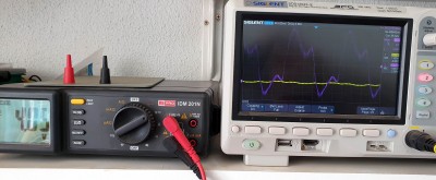
Here's a picture of the '816 on running at 36Mhz at 4.05V. The clock signal is in purple - the yellow trace is zero. The scale is 1V per div and 10ns per div.

Attachment:
20221205_084929.jpg
20221205_084929.jpg [ 176.63 KiB | Viewed 780 times ]
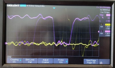
And another picture of address line 0 in purple and data line 0 in yellow. Honestly the address bus signals are really clean given the mess of noise and wire on my board. The yellow trace (being mostly driven by the Alliance SRAM) could probably be a bit better but it's hard to tell what is real and what is 'scope limitations.

plasmo wrote:
I now have faster RAM (10nS) and fast single-gate buffer so it may be interesting to repeat my overclock experiment. I'm afraid of 10nS RAM! 10nS at 5V is nightmare, so I may need to do 3-D stacking to minimize the wire length. That was something I've done with Z80, more for visual effect than control impedance consideration.
Bill
I'm really looking forward to seeing what can be done with this! Already knowing that the target overclocked frequency I want to use is about half of what can be achieved is quite comforting.

I saw your Z80 stackup way back when you first posted and thoroughly liked it. I still do :D but I think if I tried something like that I'd end up with soldering iron in the eye...

(also your post has reminded me I still need to test outside of bank 0.)

Cheers,
Andrew


Top
 Profile  
Reply with quote  
PostPosted: Mon Dec 05, 2022 8:08 am 
Offline
User avatar

Joined: Thu Dec 11, 2008 1:28 pm
Posts: 10793
Location: England
Interesting findings - and very important to see that two different short test programs have different maximum frequencies. It's an unsolved problem, to truly speed-test a microprocessor without knowing details of the internals. At minimum you'd need to be making use of every opcode, but also there will be data-dependent paths, and possibly interactions between one instruction and the next, and possibly interactions with a worst-case interrupt, or RDY. You can see the combinatorial explosion!

What you can say, of course, is that the specific program you tested ran at such and such a speed. A Basic benchmark would be fairly non-trivial, but again would really only be testing one case.


Top
 Profile  
Reply with quote  
PostPosted: Mon Dec 05, 2022 1:40 pm 
Offline

Joined: Fri Dec 21, 2018 1:05 am
Posts: 1076
Location: Albuquerque NM USA
AndrewP wrote:
plasmo wrote:
I think you've done a great job getting to 40MHz at 4V
Thanks! But I probably didn't. Not in a significant way :cry: . I was posting very early this morning whilst being eaten by mosquitoes and sitting in the dark because of being woken by loadshedding. Not a good idea.


Grew up in the subtropic without air conditioning and being served as favorite food of local mosquitos, I have a sinking feeling history may repeat itself 60 years later.

I think your signals look very clean. Scope and instrumentation can introduce unwanted artifacts especially at that frequency. 36MHz at 4V is very good, quite inspiring actually. I'm digging around for parts to see how I can repeat the overclocking test.

When overclocking CRC65, I checked the hardware with Klaus' functional test mainly because it has good coverage and fairly easy to interface.
Bill


Top
 Profile  
Reply with quote  
PostPosted: Mon Dec 05, 2022 1:49 pm 
Offline
User avatar

Joined: Thu Dec 11, 2008 1:28 pm
Posts: 10793
Location: England
Klaus' functional test is a nice idea - even better, if practical, would be Wolfgang Lorenz' test suite, which tests all opcodes with all operands. For links, and more, see 6502TestPrograms


Top
 Profile  
Reply with quote  
PostPosted: Tue Dec 06, 2022 9:08 am 
Offline

Joined: Thu Mar 03, 2011 5:56 pm
Posts: 277
Might be an idea to test some of the RMW instructions, as well as the block move instructions - these have caused a certain amount of trouble for the C256Foenix.


Top
 Profile  
Reply with quote  
PostPosted: Tue Dec 06, 2022 10:13 am 
Offline
User avatar

Joined: Mon Aug 30, 2021 11:52 am
Posts: 251
Location: South Africa
plasmo wrote:
Klaus' functional tests...
BigEd wrote:
rwiker wrote:
RMW instructions, as well as the block move instructions
Thanks! All good suggestions and definitely something I should have thought of doing.

I want to do both that and add a few more posts on what the various parts of the Bodge Board do. Unfortunately I'm a bit at the mercy of loadshedding again. It looked like things were - if not great - at least consistent for a while. But South Africa managed to misplace another 4GWatts of generation capacity, that's on top of the 16 we're already short, so we're running about 8 to 9 hours without power per day :| . Makes an electronics hobby ... challenging.


Top
 Profile  
Reply with quote  
PostPosted: Tue Dec 06, 2022 6:10 pm 
Offline
User avatar

Joined: Mon Aug 30, 2021 11:52 am
Posts: 251
Location: South Africa
I'm thinking to add descriptions of the various bits of the 816 Bodge Board (still thinking because they are quite a bit of effort to annotate).

Below are the important pieces of the board, i.e. what is needed to run the '816. I'm not going to do long textual posts because a picture is worth a thousand words. And a picture with words on it must be worth a thousand words plus words. Or something.

Attachment:
816 Bodge Board V1 - important stuff.png
816 Bodge Board V1 - important stuff.png [ 1.81 MiB | Viewed 635 times ]

I'm thinking to not use schematics because I think they're hard to read and easy to ignore. They're also hard to annotate. I find it far more interesting to see the actual PCB.

Hopefully this also means more knowledgeable members of the forum can see and comment on mistakes and also members who haven't tried putting things on PCBs yet can see it really isn't to be feared and that mistakes can be corrected (with superglue, wire and a Stanley knife).

Cheers,
Andrew


Top
 Profile  
Reply with quote  
PostPosted: Tue Dec 13, 2022 3:01 pm 
Offline
User avatar

Joined: Fri Dec 11, 2009 3:50 pm
Posts: 3346
Location: Ontario, Canada
AndrewP wrote:
I'm thinking to not use schematics [...] I find it far more interesting to see the actual PCB. [...] Hopefully this also means more knowledgeable members of the forum can see and comment on mistakes

I enjoyed your travelogue in the attached image, Andrew, but you need to give your head a shake if you think the explicitness of a schematic can be dispensed with. It's by far the most efficient way to communicate with others. And YMMV, but in my experience it's also helpful for communicating with ones self... by which I mean that creating and viewing the schematic is a valuable aid in thinking about the design.

I will comment on one point from the attached image. RDY does need to be pulled high, but, on WDC CPUs, RDY is bidirectional, and may decide to act as an output. It's better to pull high through a resistor, rather than tying straight to VCC. That's to avoid excessive current flow in the event that a WAI instruction executes, accidentally or otherwise.

-- Jeff

_________________
In 1988 my 65C02 got six new registers and 44 new full-speed instructions!
https://laughtonelectronics.com/Arcana/ ... mmary.html


Last edited by Dr Jefyll on Tue Dec 13, 2022 10:54 pm, edited 2 times in total.

Top
 Profile  
Reply with quote  
Display posts from previous:  Sort by  
Post new topic Reply to topic  [ 17 posts ]  Go to page 1, 2  Next

All times are UTC


Who is online

Users browsing this forum: No registered users and 22 guests


You cannot post new topics in this forum
You cannot reply to topics in this forum
You cannot edit your posts in this forum
You cannot delete your posts in this forum
You cannot post attachments in this forum

Search for:
Jump to: