To us, it appears that the CPU core in the 6509 and 8501 is somewhat identical to the 6502 at the logic design point of view,
just with some variations in the chip layout.
The only difference we were able to spot is in "16) PHI1# driver".
Two PHI1# metal traces are going from "16) PHI1# driver" into "17) control latch\driver".
IN the 6502, IIRC we have two inverting super buffers fed by PHI1, separately driving each of the PHI1# traces.
In the 6509\8501 we have just one (bigger) inverting super buffer fed by PHI1, driving both PHI1# traces.
Like the 6530, the 6502 is an incredibly compact beast, and it's sometimes difficult to tell
where one function block ends and the next function block starts when just staring at the silicon.
It's very impressive, that the designers were able to get two manually routed chips of that size and complexity
done and running within only a year.
6502 is a work of true art\craftsmanship, and
the designers had pulled every trick possible
to make it as compact as possible, because the size of a chip directly affects the sales price of a chip.
As in "one square millimeter of processed silicon is more expensive than one square millimeter of processed gold".
;---
Now about said tricks:
Before the 6502, the control circuitry of a CPU just was a big lump of random logic.
6502 uses a PLA (fed by the instruction Byte and the sequencer), with some random logic attached to it.
The sequencer is split into two parts.
One part (below the East end of the PLA) does the steps T0 (ALU data operation) and T1 (instruction fetch),
the other part (below the West end of the PLA) does the steps T2..T5.
When the interrupt logic detects RES#\NMI#\IRQ#, it forces the Byte from an instruction fetch to $00,
and $00 is instruction BRK, a software interrupt.
While the rest of the CPU executes the faked BRK instruction, the interrupt logic blocks PC increment
and "injects" the interrupt vector into the CPU internal address bus.
The next thing is, that BRK has one more step than the rest of the instructions: T6.
The T6 state flipflop is not part of the sequencers, on the chip it almost looks like an integral part of the interrupt logic.
Step T6 is triggered from the PLA after step T5 during a BRK instruction.
Also, the PLA does not check T6 state, so what has to be done during step T6 is defined in the random logic area.
RMW (read/modify/write) operations, that's incrementing/decrementing/shifting memory,
"fork" from the sequencer by using a flipflop "step chain" controlled by RDY,
everything related to this is deep inside the random logic area.
In my opinion, it all was intentionally build that way to minimize chip space.
;...
It is normal to have the FETs of a single logic gate "spread over half of the chip",
and it is normal that it turns out to be an AND/NOR combination gate.
It is normal to have transparent latches and NOR based RS flipflops which don't appear as such at first sight.
It also is normal to encounter logic design tricks like that one:
Attachment:
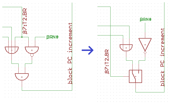 6509_mux_evil.png [ 8.73 KiB | Viewed 2949 times ]


