6502.org Forum  Projects  Code  Documents  Tools  Forum
It is currently Sat May 18, 2024 8:22 pm

All times are UTC


Post new topic Reply to topic  [ 11 posts ] 
Author Message
PostPosted: Wed Apr 28, 2021 11:18 pm 
Offline
User avatar

Joined: Sat Sep 29, 2012 10:15 pm
Posts: 899
Good news everyone! Another W65C02 is up and running.

After 3D-printing a few wire-wrap sockets (http://forum.6502.org/viewtopic.php?f=4&t=2029&p=83239#p83238), I was itching to put them to use. I always wanted to wire-wrap a computer - it seems like relaxing activity much like knitting... And I've never put together a real '02 computer, only FPGA-based, which somehow does not feel real. That's two marks on my bucket list.

The new computer is a subset of Garth's http://wilsonminesco.com/6502primer/potpourri.html#BAS_CPU (misappropriated by Mr. Eater of googletube), and the board was dubbed GARTH-1. Thank you, Garth, for a solid, simple design - and the rest of the primer!
Attachment:
garth-1.top.jpg
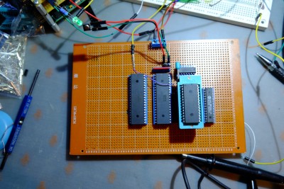
garth-1.top.jpg [ 438.37 KiB | Viewed 795 times ]

Attachment:
File comment: Bottom wire-wrap view of GARTH-1
garth-1.bot.jpg
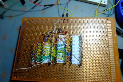
garth-1.bot.jpg [ 501.61 KiB | Viewed 795 times ]


Since I lose everything I ever write down sooner or later, I am posting some details, as much for my future self as for anyone interested:

Currently on-board:
CPU: W65C02
ROM: ATM28C256
RAM: UM61m256K-15 (skinny 32K RAM)
IO: W65C22N (I could not find an S in my pile - for some reason I bought a bunch of N's a few years back)

There is a resistor array for all the pullups, and a little header with a microscopic MCP100T SOT23-3 reset supervisor. There is a reset button floating in the air near the LED.

The cheap Chinese ZIF socket works like a charm, but unfortunately, instead of pins, has weird flat tabs that run like this:
l l l l
l l l l
They don't fit into sockets. I finally found a female header that took them, so the structure is now 3-stories high. But it works.


Clocking

I don't have a proper clock yet as all my oscillators seem to be in the tens of MHz from my FPGA days. In the meantime I've been using an Daryl's SBC4 to bang out the clock for its little brother (the LED you see is actually the clock, with a little wire to clock GARTH-1). I am running tests at around 500KHz.

Build notes:

Overall, the build took a day and a half (largely due to my disorganized space and time wasted looking for various chips and caps...). Wire-wrapping is not quite like knitting as you really have to pay attention to each individual connection, by the way. But very pleasant, and oh so retro, especially with appropriate period music. I finally got to use the little roll of Kynar wire I bought as a teenager and managed to not get rid of, somehow.

I started with the CPU and a NOP-generator stuck into the RAM socket. After banging on the knobs of my broken Kukusui 20MHz scope (the traces seem to move up and down on their own, and break up into spectacular patterns, not very helpful in debugging) I figured that it probably works. I added a ROM and loaded a simple dead loop at $FF00, which let me check the address bus lines. I then added the RAM, and burned a ROM with a simple test that JSRs into the RAM which promptly RTSs to the stable dead loop at $FF00 for verification.

Finally I added what I thought was the 6522 (but was a 6521!), and wasted half a day debugging every component, removing everything and going back to the NOP generator... Eventually I slapped my forehead and put a real 6522 in, and blinked some LEDs.

Software development

I use Linux, of course.

I use the 64TASS assembler, outputting a 64K binary. I then run dd to trim off the low 32K. It's a good thing I can use dd - otherwise I would have to wait for Balena Etcher people to hire 10 more people and make another award-winning 80MB application! There is probably a better way to generate the binary image of the upper 32K, but I haven't found it yet.

I then burn the EEPROM using my $50 XGecu Pro and minipro open-source software.

Here is my Makefile:
Code:
default:
   64tass test.asm  --flat --list=test.lst --labels=test.lab -o test.bin
   dd if=test.bin of=test.32k ibs=32768 skip=1

burn:
   minipro -p AT28C256 -w test.32k

clean:
   @rm -f *.hex *.lst *.out *.lab *.bin *.32k
   @echo "Clean!"

_________________
In theory, there is no difference between theory and practice. In practice, there is. ...Jan van de Snepscheut


Last edited by enso on Thu Apr 29, 2021 12:30 am, edited 1 time in total.

Top
 Profile  
Reply with quote  
PostPosted: Thu Apr 29, 2021 12:02 am 
Offline
User avatar

Joined: Sat Sep 29, 2012 10:15 pm
Posts: 899
The Address Decoder
Code:
74HC00 Quad 2-input NAND gate.

         +---+--+---+                 +---+---*---+           __
      1A |1  +--+ 14| VCC             | A | B |/Y |      /Y = AB
      1B |2       13| 4B  A15         +===+===*===+
     /1Y |3       12| 4A  A15         | 0 | 0 | 1 |
ϕ2    2A |4  7400 11| /4Y /ROM        | 0 | 1 | 1 |
/ROM  2B |5       10| 3B  /ROM        | 1 | 0 | 1 |
/RAM /2Y |6        9| 3A   A14        | 1 | 1 | 0 |
     GND |7        8| /3Y  /IO        +---+---*---+
         +----------+

/RAM -> RAM /CS
A14  -> RAM /OE
/ROM -> ROM /CS and /OE
/IO  -> 6522 /CS
A13  -> 6522 CS

RAM: $0000 - $3FFF
IO:  $4000 - $7FFF
ROM: $8000 - $FFFF

6522 is selected with IO and A13, and therefore mapped at $4000 + $2000


The first gate is unused for now, and I should really ground the inputs...

_________________
In theory, there is no difference between theory and practice. In practice, there is. ...Jan van de Snepscheut


Last edited by enso on Thu Apr 29, 2021 9:11 pm, edited 1 time in total.

Top
 Profile  
Reply with quote  
PostPosted: Thu Apr 29, 2021 5:35 am 
Offline
User avatar

Joined: Thu May 28, 2009 9:46 pm
Posts: 8190
Location: Midwestern USA
Excellent! A "junkpile" computer, and it actually works! :D

_________________
x86?  We ain't got no x86.  We don't NEED no stinking x86!


Top
 Profile  
Reply with quote  
PostPosted: Thu Apr 29, 2021 3:04 pm 
Offline
User avatar

Joined: Sat Sep 29, 2012 10:15 pm
Posts: 899
Still can't find any reasonable oscillators in my vast junkpile.

I am still using Daryl Ricter's SBC4 as a clock source. I was thinking the optimum pin-twiddling loop when I remembered that the 6522 can use a timer to twiddle the pin. Fastest I can go, setting the count to 0, PB7 should output 1/4 of the SBC4's clock. I think SBC4 runs at 10MHz (Daryl - am I right? The can on the SBC4 is covered with expansion boards and I can't see it), so I should be getting 2.5MHz.

Code:
; 68C816 on SBC4:
  LDA   #%11000000
  STA   ACR
  STZ   T1CL
  STZ   T1CH


And it's outputing a square wave, roughly 4 times faster than before, which makes sense. GARTH-1 is keeping up, flashing the LED much faster. Sanity check: using the delay from the primer:
Code:
;; 65C02 on GARTH-1
;; 9*(256*A+Y)+8+12 cycles
delay:
        CPY  #1
        DEY
        SBC  #0
        BCS  delay
        rts

With $FF in A and Y, we should blow 589835 cycles between LED toggles. I don't have a stopwatch handy, but it looks like maybe about 2 blinks (4 delays) per second. That comes out to a bit under 2.5MHz.

Shift Register?
Quote:
2.13.1 Shift Out - Free Running at T2 Rate (100)
This mode is similar to mode 101 in which the shifting rate is determined by T2. However, in mode
100 the SR Counter does not stop the shifting operation. Since SR7 is re circulated back into SR0,
the eight bits loaded into the SR will be clocked onto the CB2 line repetitively. In this mode, the SR
Counter is disabled and IRQB is never set...
...
2.13.3 Shift Out - PHI2 Clock Control (110)
In this mode, the shift rate is controlled by the system PHI2 clock.

PHI2 mode unfortunately is destructive... SR will need to be reloaded, which blows. The free running mode cannot go faster than 2 clocks per transition, same as above. Darn.

I have one final trick left: I can grab PHI2 from the SBC4's expansion bus... And it runs at 10MHz!

I figured the ROM would not make it to 10MHz... An I am pulling PHI2 from the SBC across a foot of hookup wire. My scope shows it as a sine wave. I really should get a Rigel. But it's pretty impressive.

_________________
In theory, there is no difference between theory and practice. In practice, there is. ...Jan van de Snepscheut


Top
 Profile  
Reply with quote  
PostPosted: Thu Apr 29, 2021 4:25 pm 
Offline
User avatar

Joined: Fri Dec 11, 2009 3:50 pm
Posts: 3354
Location: Ontario, Canada
enso wrote:
The free running mode cannot go faster than 2 clocks per transition
Huh! I thought you were mistaken on this point, but I see it's true. For some reason Mode 4 (the free-running mode) is half the speed of the (otherwise highly similar) Modes 2 and 3. I never noticed that before.

Quote:
I have one final trick left: I can grab PHI2 from the SBC4's expansion bus...
Yup. Or, instead of grabbing Phi2, you could get Phi2 divided by 2, by 4, by 8 etc from the LS lines of the address bus. Just put SBC4 in a loop something like this: :)

Code:
Looptop: CMP #0
         CMP# 0
         CMP #0
         CMP #0
         CMP #0
         JMP inline
inline:  JMP Looptop

-- Jeff

_________________
In 1988 my 65C02 got six new registers and 44 new full-speed instructions!
https://laughtonelectronics.com/Arcana/ ... mmary.html


Top
 Profile  
Reply with quote  
PostPosted: Thu Apr 29, 2021 7:26 pm 
Offline
User avatar

Joined: Sat Sep 29, 2012 10:15 pm
Posts: 899
Well, it's pretty solid at 10MHz. I am surprised, given the flaky clock connection and the noticeable clock frequency on the powerline. I really need to clock this computer. No reason to downgrade yet.

_________________
In theory, there is no difference between theory and practice. In practice, there is. ...Jan van de Snepscheut


Top
 Profile  
Reply with quote  
PostPosted: Fri May 14, 2021 12:50 am 
Offline
User avatar

Joined: Sat Sep 29, 2012 10:15 pm
Posts: 899
10MHz is as fast as it can go.

12MHz (24MHz oscillator fed through a flop) is too much.

AT21C256 is the slowest chip in my system. I tried a few different ones, as I mixed up some from Mouser with others from god knows where. I found some slower ROMs: 3 similarly marked ones only work at 8MHz. All three slow chips have the following markings:

AT21C256F
15PI
1612

Curious: I have a few 20PI chips that work at 10MHz.

Well, 10MHz is not too bad. The current decoder uses A15 to /CS and /OE the ROM. At 10MHz we technically have 50ns for the read half-cycle, although if the address bus is set up a little earlier, possibly a tiny bit more. So using 150ns (and even 200ns) devices is pushing it.

_________________
In theory, there is no difference between theory and practice. In practice, there is. ...Jan van de Snepscheut


Top
 Profile  
Reply with quote  
PostPosted: Sun May 16, 2021 3:40 am 
Offline
User avatar

Joined: Sat Sep 29, 2012 10:15 pm
Posts: 899
I equipped the board with a full-can oscillator in a 14-pin socket. I probably should've gone with half-can but couldn't resist.

I love the feel of the full-can! In the past decade I've mostly used surface-mount 5x7mm parts which weigh nothing. The full-can oscillator has a definite heft. It feels like the source of real computing power.

_________________
In theory, there is no difference between theory and practice. In practice, there is. ...Jan van de Snepscheut


Top
 Profile  
Reply with quote  
PostPosted: Fri May 21, 2021 11:06 am 
Offline
User avatar

Joined: Tue Aug 11, 2020 3:45 am
Posts: 311
Location: A magnetic field
enso on Thu 29 Apr 2021 wrote:
Code:
    +---+--+---+
 1A |1  +--+ 14| VCC
 1B |2       13| 4B  A15
/1Y |3       12| 4A  A15


...

The first gate is unused for now, and I should really ground the inputs...


It is possible to tie together pin 1, pin 2, pin 13 and pin 14.

_________________
Modules | Processors | Boards | Boxes | Beep, Beep! I'm a sheep!


Top
 Profile  
Reply with quote  
PostPosted: Fri May 21, 2021 3:33 pm 
Offline
User avatar

Joined: Thu May 28, 2009 9:46 pm
Posts: 8190
Location: Midwestern USA
Sheep64 wrote:
enso on Thu 29 Apr 2021 wrote:
Code:
    +---+--+---+
 1A |1  +--+ 14| VCC
 1B |2       13| 4B  A15
/1Y |3       12| 4A  A15


...

The first gate is unused for now, and I should really ground the inputs...

It is possible to tie together pin 1, pin 2, pin 13 and pin 14.

Better is to pull up unused inputs to Vcc with individual resistors. That way, the inputs can be pressed into service at a later time if needed. A 3.3K, bused SIP resistor pack is good for this purpose due to its compactness.

_________________
x86?  We ain't got no x86.  We don't NEED no stinking x86!


Top
 Profile  
Reply with quote  
PostPosted: Sat May 22, 2021 1:21 am 
Offline
User avatar

Joined: Sat Sep 29, 2012 10:15 pm
Posts: 899
BigDumbDinosaur wrote:
A 3.3K, bused SIP resistor pack is good for this purpose due to its compactness.

I have a few hundred of those. Good advice.

_________________
In theory, there is no difference between theory and practice. In practice, there is. ...Jan van de Snepscheut


Top
 Profile  
Reply with quote  
Display posts from previous:  Sort by  
Post new topic Reply to topic  [ 11 posts ] 

All times are UTC


Who is online

Users browsing this forum: No registered users and 3 guests


You cannot post new topics in this forum
You cannot reply to topics in this forum
You cannot edit your posts in this forum
You cannot delete your posts in this forum
You cannot post attachments in this forum

Search for:
Jump to: