6502.org Forum  Projects  Code  Documents  Tools  Forum
It is currently Wed May 15, 2024 2:15 pm

All times are UTC


Post new topic Reply to topic  [ 192 posts ]  Go to page Previous  1, 2, 3, 4, 5, 6, 7 ... 13  Next
Author Message
PostPosted: Sun Oct 06, 2019 2:40 pm 
Offline

Joined: Fri Jan 25, 2019 2:29 pm
Posts: 192
Location: Madrid, Spain
Attachment:
WhatsApp Image 2019-10-06 at 16.28.40.jpeg
WhatsApp Image 2019-10-06 at 16.28.40.jpeg [ 111.62 KiB | Viewed 1769 times ]
Attachment:
WhatsApp Image 2019-10-06 at 15.01.56.jpeg
WhatsApp Image 2019-10-06 at 15.01.56.jpeg [ 108.64 KiB | Viewed 1769 times ]


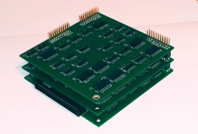
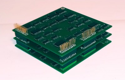
Finally, B1 and B2 are completed and they.... kinda work... Although I'm going to have to check quite a few things.

Remember how B0 performed flawlessly, both when connected via the expansion port, and when replacing CIA#2? Well, that's no longer true. I'm getting weird image artifacts when doing that, even using only B0. All registers work OK when connected into the expansion port, so it seems something's wrong with the port outputs. Until I figure it out, I'll do only testing via the expansion port.

Now, about the new boards, I've only been able to do some limited testing. Timers start and stop, and the do count as expected. B0+B1 work, B0+B2 work too. However, if I connect the whole stack (B0+B1+B2) my C64 starts to behave weirdly. I get no cursor and no keyboard. This implies CIA#1 no longer works. I get the startup screen, and Run/Stop+Restore does what it should, so CPU, VIC.. they are pretty much OK. I may be drawing too much power and CIA#1 is the first victim, or some other signal may be being affected.

Something I didn't take into account is how many inputs can I drive from the C64 outputs, and I'm maybe paying for that now.

So, plan for the next couple of weeks. Run some extensive testing on both timers individually, identify why B0 seems not to work properly on its own, and find what's going on when I connect the full stack.

After an uninterrupted successful streak of 14 months, with no issues at all, this feels weird but... It couldn't be so easy :)

Cheers!


Last edited by daniMolina on Wed Oct 09, 2019 3:04 pm, edited 1 time in total.

Top
 Profile  
Reply with quote  
PostPosted: Mon Oct 07, 2019 10:37 am 
Offline
User avatar

Joined: Fri Nov 09, 2012 5:54 pm
Posts: 1394
Sorry to hear this.

From the C64 schematics:
D7..0, A3..0, R/W, PHI2 and /RES signals are supposed to be identical for both of the CIA sockets and the expansion port.
CIA2 generates the (edge sensitive) /NMI signal, and I think that /NMI stuck LOW isn't supposed to stop the C64 BASIC+KERNAL (when not emulating RS232).

CIA2 does generate /VA14 and /VA15 (through PA0 and PA1), something wrong there _could_ explain odd artefacts on the screen.

From the datasheet, 6526 is supposed to draw 70mA..100mA from the power supply, and I would recommend to check this first.
//But it's somewhat unlikely that something like a handful of 74HCT chips running at ca. 1MHz draws more than 100mA from the power supply.

I also would recommend an "optical inspection" of B0 just to be sure that no short circuit had happened by accident,
something like a little piece of solder that went between two SMD chip pins during the building process.

If this won't help, it would be worth to check if B0 emits something on the data bus when it shouldn't.

Edit:
Say... aren't there supposed to be 100nF SMD capacitors soldered into the power supply on these PCBs ?
I fail to see them in your pictures... please check, because _if_ they are missing this could explain those problems.


Top
 Profile  
Reply with quote  
PostPosted: Mon Oct 07, 2019 12:16 pm 
Offline
User avatar

Joined: Fri Dec 11, 2009 3:50 pm
Posts: 3354
Location: Ontario, Canada
daniMolina wrote:
they.... kinda work
I'm wondering, is the behavior intermittent? Does the thing work and then not work, seemingly at random? If that's the case I can think of some suggestions.

But in any case do consider Dieter's remark about bypass capacitors. :wink:

-- Jeff

_________________
In 1988 my 65C02 got six new registers and 44 new full-speed instructions!
https://laughtonelectronics.com/Arcana/ ... mmary.html


Top
 Profile  
Reply with quote  
PostPosted: Tue Oct 08, 2019 5:48 am 
Offline
User avatar

Joined: Fri Nov 09, 2012 5:54 pm
Posts: 1394
daniMolina wrote:
All registers work OK when connected into the expansion port

How you are connecting the 74HCT6526 to the expansion port or the CIA sockets ?

I suppose, that you are plugging the 74HCT6526 more or less directly to the expansion port,
and that you are using ribbon cables (flat cables) for plugging the 74HCT6526 to a CIA socket.

How long are those ribbon cables ?
Is every second wire in the cable GND (like with old floppy cables) for preventing crosstalk between the signal wires ?
Sending the data bus of a 1MHz NMOS 6502 computer through, let's say, 10 centimeters of ribbon cable without making
every second wire of the cable GND already might do for affecting the reliability of the system.

Please check.


Top
 Profile  
Reply with quote  
PostPosted: Tue Oct 08, 2019 11:40 am 
Offline

Joined: Fri Jan 25, 2019 2:29 pm
Posts: 192
Location: Madrid, Spain
Thank you all for your replies and all the information!

Right now, my main suspects are VDD or PHI2.

VDD, The pads for all bypass caps are in the PCBs, but no, I haven't soldered them. I wanted to check how much of an effect did they have, so I completely skipped them on B0. Everything worked fine then, so I just ignored them, until now. I've been pointed in this direction by several other people

VDD, although unlikely, I may be drawing too much power (around 75 ICs with the full stack so far)

PHI2, is being fed into 18 inputs. I need to do some numbers to find out how much current this requires, and if this is OK for my CPU right now.

There could be plenty of other reasons, of course, a bad contact or solder point, a short of some kind, maybe some error in design where I'm connecting stuff I shouldn't.

As soon as I can, I'll be taking a good bunch of measures with my oscilloscope.


Last edited by daniMolina on Wed Oct 09, 2019 3:06 pm, edited 1 time in total.

Top
 Profile  
Reply with quote  
PostPosted: Tue Oct 08, 2019 7:53 pm 
Offline

Joined: Fri Jan 25, 2019 2:29 pm
Posts: 192
Location: Madrid, Spain
Well... it was easier than I thought... At least, finding what's causing my problems. Fixing them, still unknown.

I'm definitely trashing PHI2. This is PHI2, with no weirdos attached
Attachment:
sensitivity_10x.PNG
sensitivity_10x.PNG [ 15.06 KiB | Viewed 1669 times ]


Adding B0
Attachment:
sensitivity_10x_b0.PNG
sensitivity_10x_b0.PNG [ 17.07 KiB | Viewed 1669 times ]


Adding B1
Attachment:
sensitivity_10x_b0_b1.PNG
sensitivity_10x_b0_b1.PNG [ 17.9 KiB | Viewed 1669 times ]


Adding B2
Attachment:
sensitivity_10x_b0_b1_b2.PNG
sensitivity_10x_b0_b1_b2.PNG [ 18.78 KiB | Viewed 1669 times ]


The more things I have feeding on PHI2, the longer it takes to raise.

Interestingly enough, connecting just the scope with the sensitivity set to x1, is causing the same effect.
Attachment:
sensitivity_1x.PNG
sensitivity_1x.PNG [ 13.96 KiB | Viewed 1669 times ]


BTW, I haven't seen anything out of normal on Vdd. All three boards together draw 6.3 mA. Removing boards one by one, shows each board drawing between 2, 2.3 mA each.

Now I'll add bypass caps and, if nothing changes, I'm thinking about running PHI2 through a buffer.

Heating my soldering iron!


Last edited by daniMolina on Wed Oct 09, 2019 3:08 pm, edited 1 time in total.

Top
 Profile  
Reply with quote  
PostPosted: Tue Oct 08, 2019 10:28 pm 
Offline

Joined: Mon May 21, 2018 8:09 pm
Posts: 1462
Yeah, old machines like the C64 typically use 74LS logic which has much higher pull-up impedance than pull-down. The important area, fortunately, is below the TTL Vih threshold of about +2.4V, but even here you have enough loading to change the slope of the signal noticeably. So the signal spends more time in the ambiguous zone between Vil and Vih, which can be seen by logic as rapid glitches.

Inserting a 74HCT buffer in the clock line should reduce the load on the C64's clock to a single CMOS input, and the CMOS output will have no trouble driving everything you want.


Top
 Profile  
Reply with quote  
PostPosted: Wed Oct 09, 2019 6:24 am 
Offline
User avatar

Joined: Fri Nov 09, 2012 5:54 pm
Posts: 1394
Basically, a 74HCT input is supposed to have 5pF..10pF of capacitance to GND.
When increasing the capacitive load on the PHI2 line by adding a lot of 74HCT inputs to it, PHI2 needs more time to rise to HIGH level.

Logic level threshold for 74HCT inputs is supposed to ba ca. 1.3V, and like Chromatix has pointed out,
it's an interesting question if 74HCT inputs might be getting "confused" if the rising edge of PHI2 goes through that voltage level too slowly.

Try running PHI2 through a buffer, preferably a 74HCT245, because the 74HCT245 might be a better choice for driving capacitive loads than the average 74HCT logic gate.
//When trying to aim for a higher PHI2 clock rate later, try to keep in your backhead that the buffer has a propagation delay.


About the effects on PHI2 with x1 scope sensivity... the probe, the cable and the scope input also add some capacitive load to PHI2.
A picture from somewhere at the start of this thread:

Image

//There might be some more problems hiding below the surface of course, but on the bright side you are not in a hurry for fixing them.


Top
 Profile  
Reply with quote  
PostPosted: Wed Oct 09, 2019 8:46 pm 
Offline

Joined: Fri Jan 25, 2019 2:29 pm
Posts: 192
Location: Madrid, Spain
A single buffer did the trick!

I'll add anyway the bypass caps, then can't do any harm.

Next task, prepare an intensive test suite for the timers :)


Top
 Profile  
Reply with quote  
PostPosted: Fri Oct 11, 2019 5:54 am 
Offline
User avatar

Joined: Fri Nov 09, 2012 5:54 pm
Posts: 1394
Would be interesting to count the 74HCT inputs\outputs tied to D7..0, A3..0, R/W in your 74HCT6526,
then to multiply the result by two (because the C64 has two CIAs).

Looking forward to see, how the timer testing turns out.


Top
 Profile  
Reply with quote  
PostPosted: Fri Oct 11, 2019 11:18 am 
Offline

Joined: Fri Jan 25, 2019 2:29 pm
Posts: 192
Location: Madrid, Spain
ttlworks wrote:
Would be interesting to count the 74HCT inputs\outputs tied to D7..0, A3..0, R/W in your 74HCT6526,
then to multiply the result by two (because the C64 has two CIAs).


That's actually already defined, even though there are two boards which aren't even designed.

Each data pin goes into 3 inputs, but I have a change in mind that would reduce it to just 1.
Each Address line, into 2 inputs (Two chained 74138 3-8 decoders). Same for /CS (Also, each CIA receives a different /CS from the PLA)
R/W just one input in the whole stack.

*Should* be OK, if they have the same strength as PHI2


Top
 Profile  
Reply with quote  
PostPosted: Fri Oct 11, 2019 12:12 pm 
Offline

Joined: Mon May 21, 2018 8:09 pm
Posts: 1462
Yeah, that sounds fine. A 74HCT input is less of a load than a 74LS input, so it's okay to replace one TTL load with a small number of CMOS loads.

I gather the clock line went to a much larger number of places.


Top
 Profile  
Reply with quote  
PostPosted: Sat Oct 12, 2019 9:23 pm 
Offline

Joined: Fri Jan 25, 2019 2:29 pm
Posts: 192
Location: Madrid, Spain
Chromatix wrote:
I gather the clock line went to a much larger number of places.


Around 20 inputs I'd say. With B0+B1, or B0+B2 it still worked (10-12 inputs) but PHI2 was already very much affected. Anyway, a buffer for the clock will be added for the second revision of the board. For the tests with the current board, I'm using a single gate 125 I had lying around. It doesn't look so nice as before, but so far, it's doing its job.

A brief heads up on timer testing. I've spent quite a few hours this weekend here
Attachment:
test_Setup.jpeg
test_Setup.jpeg [ 166.32 KiB | Viewed 1550 times ]


It's starting to look a lot like my bedroom when I was a kid, not sure if that's good or bad though... :D

Using a small piece of assembly that took me 2 hours to complete (I've got so rusty)

Attachment:
live_view.jpeg
live_view.jpeg [ 222.33 KiB | Viewed 1550 times ]


I've been able to try plenty of stuff. There are some things remaining that will need some heavy use of my logic analyzer, as timing's crucial.

The good news so far :
  1. Starting values. Timers' latches should be set to 1, control register to 0. Big facepalm here, as I completely messed up the schematics, a (very much) needed inverter is missing. As a consequence, Timers' latches are perpetually set to 1. Some PCB hacking has been done and, now they initialize with rubbish, but at least I can write to them. An easy fix for rev 2. Control registers initialize OK
  2. PB7 and PB6 override. Setting the bit in the control register forces PB6 and PB7 as outputs.
  3. Timer reloading from latches. Works fine, whenever a write to the high byte with timer is stopped, whenever FORCELOAD is written with a 1 (which is stored nowhere), or whenever there's and underflow
  4. Timer output on PB6 and 7. TIMERB toggle output works. Pulse output requires the logic analyzer to check. TIMERA output is completely missing. Circuits are the same for both timers, so could be caused by a bad solder
  5. Timer B won't count Timer A underflows. Could be related to the above issue
  6. One shot mode. It works, timer counts down until the overflow happens, Then relatches the value.... but then it ticks once more before stopping. Same for both timers.

The untested bits:
  1. Pulse output.
  2. CNT pulses counting
  3. Different overflow behavior counting PHI2 vs CNT (4-3-2-1-4-4-3-2 vs 4-3-2-1-0-4-3-2-1-0)

And the know issues:
  1. TIMERA underflow seems to fail. Could be a bad solder
  2. START bit gets set to 1 on its own sometimes. Same for both TIMERS.
  3. Adittional tick in One Shot Mode. I think this is caused by the 2 DFF feeding the clock to the Timer. When Timer stops, there more clocks in the queue. I probably need to clear one of them when the underflow is reached.

All in all... I'd say it's a 7/10 score so far. START bit has me scratching heavily my head... but I think I should better sleep on it. I've had no ideas about what's causing this so far.

Cheers!


Top
 Profile  
Reply with quote  
PostPosted: Fri Oct 18, 2019 6:25 pm 
Offline

Joined: Fri Jan 25, 2019 2:29 pm
Posts: 192
Location: Madrid, Spain
daniMolina wrote:
Adittional tick in One Shot Mode. I think this is caused by the 2 DFF feeding the clock to the Timer. When Timer stops, there more clocks in the queue. I probably need to clear one of them when the
underflow is reached.


Attachment:
clock_queue.png
clock_queue.png [ 9.55 KiB | Viewed 1512 times ]


Exactly as suspected, clock in u10a was cleared on timer underflow, but clock in u10b wasn't. (PIN13 was connected to Vcc, this is an old image).

Connecting the FORCELOAD signal to U10 pin 13, causes the clock queue to be emptied on timer underflow. In One Shot mode, timer gets reloaded and stops counting in the same cycle (expected behaviour). In continuos mode, when timer reaches 1, it reloads, skips one cycle, and keeps counting.

One more issue crossed out my list!


Top
 Profile  
Reply with quote  
PostPosted: Sat Oct 19, 2019 2:05 am 
Offline
User avatar

Joined: Sun Oct 18, 2015 11:02 pm
Posts: 428
Location: Toronto, ON
Nicely done Dani! It’s great to see persistence paying off. Cheers.

_________________
C74-6502 Website: https://c74project.com


Top
 Profile  
Reply with quote  
Display posts from previous:  Sort by  
Post new topic Reply to topic  [ 192 posts ]  Go to page Previous  1, 2, 3, 4, 5, 6, 7 ... 13  Next

All times are UTC


Who is online

Users browsing this forum: No registered users and 9 guests


You cannot post new topics in this forum
You cannot reply to topics in this forum
You cannot edit your posts in this forum
You cannot delete your posts in this forum
You cannot post attachments in this forum

Search for:
Jump to: