6502.org Forum  Projects  Code  Documents  Tools  Forum
It is currently Sun Nov 24, 2024 12:05 pm

All times are UTC


Post new topic Reply to topic  [ 52 posts ]  Go to page 1, 2, 3, 4  Next
Author Message
PostPosted: Thu Sep 29, 2016 2:18 pm 
Offline
User avatar

Joined: Fri Aug 30, 2002 1:09 am
Posts: 8546
Location: Southern California
Note: for the final spec, go to the 29th post.

Elsewhere, I recommended standardizing on a pinout for tiny I²C modules. I called it I2C-6. Daryl used it on at least one of his SBCs that he sells. Below is a recommendation for a similar type for SPI, equally hobbyist-friendly, using standard pin headers of .025" square posts with pin spacing at .100". These fit into standard perfboard for wire-wrapping or soldering.

Background

I²C and SPI are synchronous-serial interfaces that are very popular because they dramatically reduce the number of required connections compared to parallel. (There are other very similar, lesser-used ones too, like SMBus and Microwire.) Besides the fact that they make computer construction easier, once you have an I²C and/or SPI interface in place, a 6502 with only a 64KB memory map can access lots of ICs on the serial buses, and even megabytes (or gigabytes) of flash memory, without complex address decoding or banking. Many of the ICs have only 8 pins. Putting D/A and A/D converters, keyboard scanners, display drivers, temperature sensors, signal generators, general-purpose I/O bits, relay drivers, real-time clocks, etc. on separate boards or modules becomes much, much easier.

I²C and SPI do not have the timing requirements that an asynchronous serial interface like RS-232 does. They are easy for the hobbyist to bit-bang with any standard I/O IC like the 6522 VIA, 6520 PIA, 6526 CIA, or non-65-family parts with similar functions. Daryl also sells his 65SPI chip which does the SPI shifting in hardware, has 8 slave-select outputs, and has a 6502-compatible bus interface. SPI needs a minimum of four signal lines (clock, data in each direction, and select) compared to I²C's two (a bidirectional data line, plus a clock line which is also potentially bidirectional), but SPI can go about a hundred times as fast because it doesn't rely on passive pull-up resistors like I²C does. All SPI lines are unidirectional, making it easy to do voltage translation if needed (like from 5V to 3.3V). There's a summary of several serial interface methods here. Thousands of ICs are available with I²C and SPI.

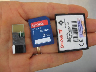
My own first application for SPI-10 is 4MB flash memories that come in a wide SO-8 package about 0.2"x0.3". Here's one of my home-made modules, and to the right, a standard SD card and a CompactFlash card. On the SPI-10 module, pin 1 is marked by a white stripe (I used white-out), and the two-pin 90° header is to put a jumper on for write-protect. 40% of the board is just there as a handle to unplug it, and/or to have a small space to label what you have stored on the module. You can make your own file system, or even use the module without any file system at all.
Attachment:
flashModuleCompare.jpg
flashModuleCompare.jpg [ 46.06 KiB | Viewed 10022 times ]

I've used this flash memory before, but only on an SO-to-DIP adapter, plugged into an 8-pin DIP socket. The SPI-10 module makes it much more convenient to insert and remove, and it won't get damaged in handling like a DIP's pins would.

The details

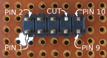
Here's a view looking down on a straight (vertical) 10-pin SPI-10 header. The pin header goes on the controller (master), while the module (slave) gets the socket, since the modules might be too vulnerable to mechanical damage if they had the pins. Pin 8 is cut as a keyway, and the corresponding hole in the module's socket is blocked to prevent inserting the module backwards or offset. Mark pin 1 in the PCB's silkscreened legend, or with white-out or a permanent marker if by hand.
Attachment:
SPI-10pinout.jpg
SPI-10pinout.jpg [ 34.85 KiB | Viewed 10022 times ]

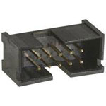
If you want a little more protection for the pins on the controller board, there's no reason you couldn't use a shrouded pin header like this one:
Attachment:
shrouded10.jpg
shrouded10.jpg [ 4.13 KiB | Viewed 10022 times ]

The picture is from a distributor's site and does not have pin 8 cut off. If it's too hard to reach into the shroud with a wire cutter, you might be able to pull the pin out from the back with needle-nose pliers.

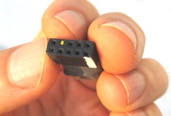
Position 8 of the module's socket is blocked, to prevent plugging it in wrong. On this one, I pulled the contact out before soldering the socket to the tiny board, and jammed a piece of wire with yellow insulation in the hole. Note the white-out marking pin 1.
Attachment:
moduleSocket.jpg
moduleSocket.jpg [ 24.17 KiB | Viewed 10022 times ]


You could put the pin header at the edge of the board as well, using 90° pins. You can flip it if desired. Here's the pinout:
Code:
      Gnd  MOSI MISO (cut) IRQ\
     ┌────┬────┬────┬────┬────┐
     │  2 │  4 │  6 │ (8)│ 10 │
     ├────┼────┼────┼────┼────┤
     │  1 │  3 │  5 │  7 │  9 │
═════╧════╧════╧════╧════╧════╧══════(board edge)
      Vdd   Clk  CS\  AUX RST\


Pin and signal descriptions:

  1. VDD. Voltage should be labeled, especially for a 5V controller port, or a lower-voltage (mostly meaning 3.3V) module. A port that is only for flash memory probably will not be 5V since AFAIK there are no SPI flash memories available in 5V.

  2. Ground

  3. Clk. SPI serial clock input to module. SPI can go as fast or slow as you like. At the high end, some devices can go up to about 200MHz. At the low end, you can even stop the clock at any time with no ill effects, even in the middle of a byte, for example to service an interrupt (although the ISR should not affect the SPI).

  4. MOSI. Master-out, slave-in serial data.

  5. CS\. Active-low chip select input to module.

  6. MISO. Master-in, slave-out serial data. SPI can run data in both directions at once, although most devices don't have any reason to.

  7. AUX. Some SPI ICs or devices have a separate pin for register select, for example a small graphics LCD I have which sees a "1" there to mean incoming bits are data and a "0" to mean they're an instruction. Use this like any way you like; but I expect that the few times it's needed, it will be an input to the slave.

  8. Empty. Pin 8 is cut off, and the hole in the socket is plugged, to prevent accidentally plugging the module in backwards or offset.

  9. RST\. Active-low reset input to the module. Most SPI ICs won't need this.

  10. IRQ\. Interrupt-request open-collector/open-drain output from the module. The module can pull this line down to request service. Use a pull-up resistor to VDD on the controller.

If you absolutely must to have a smaller module, note that the six essential connections are all together, in pins 1 through 6, so positions 7 through 10 could be left off and the module's socket could be hardly over .300" wide.

If you want it hot-pluggable, the controller should be able to turn off the power and bring its outputs low. I recommend using an LED next to the pin header on the controller board to show when the port is powered up (modern, high-efficiency LEDs only need a mA or two, not 20!), and if there's any risk of damage, you should plug in or unplug a module only when the light is off. The restriction could be eliminated with special connectors to make sure the power and ground get connected before the other lines (when plugging in) and disconnected last (when unplugging); however, a goal here is to use common, inexpensive parts that are widely available to hobbyists and can be inserted into common perfboard.

My first interest in this is for SPI flash memories. I'm starting with a board that accommodates the 25VF032 and 26VF064 4MB and 8MB flash memories and others with the same footprint (and I plan to make the board available to everyone); but SPI-10 can also serve to connect circuits centered on tons of other SPI ICs, as mentioned in the 2nd paragraph from the top.

SPI-10 does not in any way nullify 65SIB. 65SIB is a bus for multiple slaves, with auto addressing and other things that SPI-10 does not have. SPI-10 is for single-address modules that will usually be quite small.

If you see any problems, or anything needs clarification, please let me know, and I'll edit this so all the corrections will be incorporated into the head post (after discussion if necessary). Each builder can of course do things however (s)he wants; but I hope this proposed standard will not only be helpful in individuals' projects but will facilitate the sharing of projects.

_________________
http://WilsonMinesCo.com/ lots of 6502 resources
The "second front page" is http://wilsonminesco.com/links.html .
What's an additional VIA among friends, anyhow?


Top
 Profile  
Reply with quote  
PostPosted: Thu Sep 29, 2016 5:00 pm 
Offline
User avatar

Joined: Fri Dec 11, 2009 3:50 pm
Posts: 3367
Location: Ontario, Canada
Very nice! Thanks for sharing your work with us, Garth.


GARTHWILSON wrote:
If it's too hard to reach into the shroud with a wire cutter, you might be able to pull the pin out from the back with needle-nose pliers.
Yes, if you get a good grip with the pliers then usually the pin will come out easily. If it doesn't, just touch a soldering iron to it. :twisted:
Attachment:
shrouded10.jpg
shrouded10.jpg [ 4.13 KiB | Viewed 10008 times ]

_________________
In 1988 my 65C02 got six new registers and 44 new full-speed instructions!
https://laughtonelectronics.com/Arcana/ ... mmary.html


Top
 Profile  
Reply with quote  
PostPosted: Thu Sep 29, 2016 7:17 pm 
Offline
User avatar

Joined: Sun Dec 29, 2002 8:56 pm
Posts: 460
Location: Canada
I'm reminded of the Digilent PMODx2 interface which has 12 posts. For an FPGA the pinout doesn't matter that much, but the power and ground are at one end.
Pin 5,11 and 6,12 are ground and VCC. the other pins are user defined. I believe they have FLASH modules.

_________________
http://www.finitron.ca


Top
 Profile  
Reply with quote  
PostPosted: Thu Sep 29, 2016 8:11 pm 
Offline
User avatar

Joined: Fri Aug 30, 2002 1:09 am
Posts: 8546
Location: Southern California
Usually it is desirable to evenly distribute the power and ground pins among the signal pins, so any given signal line's return path is as close as possible, minimizing inductance and taking advantage of mutual inductance. I did that in my 4MB 10ns SRAM module, and SPI-10 has the same 0.2" max separation between ground and the farthest potentially fast signal line (MISO). If you touch the unshrouded pin header with your finger or tool without being grounded, you're less likely to cause static damage if the corner pins are power and ground, since they're most likely to get touched first. An intermediate step might be to put them in positions 2 and 5 instead. I must confess that my arrangement of the pins was partially influenced by what appeared to make routing the little board to the 25VF032 flash memory pinout easiest; but although I got 33 PCBs to start, the reason I'm not immediately offering them to others is that I made a mistake on the width of the IC, not realizing it was wider than a normal SO-8, so I had to bend the inverted gull-wing leads under, making the part more or less J-leaded in order to solder it. It works, but it adds to assembly labor. So if I re-do it anyway, this is the time to make changes, before there's anything substantial already in existence. I'm open to that. These modules will not normally be interfaced with cables, ribbon or otherwise, where it would become more important to have a ground or virtual ground next to every signal wire like we did with 65SIB.

Another matter that has come up (by PM) is that it's confusing which row of pins should correspond to the component side of the module. I can see where that confusion came in, and that may need some work. Further feedback is welcome. On some things like the flash memory, it doesn't matter. However, if you have things that need some human interface, for example a trimmer, LED, pushbutton, IR transmitter/receiver, etc., and the board is horizontal to a work surface, you would want those on the top.

To minimize confusion, I tried to have this as developed as possible before presenting it, but again this is the time to make any needed changes before people start making things with it.

_________________
http://WilsonMinesCo.com/ lots of 6502 resources
The "second front page" is http://wilsonminesco.com/links.html .
What's an additional VIA among friends, anyhow?


Top
 Profile  
Reply with quote  
PostPosted: Thu Sep 29, 2016 8:56 pm 
Offline
User avatar

Joined: Thu May 28, 2009 9:46 pm
Posts: 8514
Location: Midwestern USA
GARTHWILSON wrote:
Usually it is desirable to evenly distribute the power and ground pins among the signal pins, so any given signal line's return path is as close as possible, minimizing inductance and taking advantage of mutual inductance.

Any thought about assigning a pin to carry 3.3 volts to modules that use it instead of 5 volts?

_________________
x86?  We ain't got no x86.  We don't NEED no stinking x86!


Top
 Profile  
Reply with quote  
PostPosted: Thu Sep 29, 2016 9:51 pm 
Offline
User avatar

Joined: Fri Aug 30, 2002 1:09 am
Posts: 8546
Location: Southern California
BigDumbDinosaur wrote:
Any thought about assigning a pin to carry 3.3 volts to modules that use it instead of 5 volts?

The problem is that the logic levels may need to change too, not just the power supply voltage. One thing I considered briefly but quickly discounted it was that everything at the connector be 5V, and if a modules' SPI IC were 3.3V, the module would do its own voltage translations. Another idea was a pin on the module that would tell the master if it needed 3.3V instead of 5V, and then the translation and regulator circuits would only be on the master, and not replicated on every module. So far I don't see any tidy solution; but I'm open to suggestions. Many of the 5V ICs one may want to put in a module may not consistently interpret a TTL high as a logic 1. The number of SPI ICs on the market is staggering.

_________________
http://WilsonMinesCo.com/ lots of 6502 resources
The "second front page" is http://wilsonminesco.com/links.html .
What's an additional VIA among friends, anyhow?


Top
 Profile  
Reply with quote  
PostPosted: Fri Sep 30, 2016 6:10 am 
Offline
User avatar

Joined: Thu Dec 11, 2008 1:28 pm
Posts: 10986
Location: England
One could presumably make a small (2 chip) stacking converter, with a regulator and level shifters, for the 3V case? It would be interesting to know what the relative demand would be, between 5V and 3V use-cases.


Top
 Profile  
Reply with quote  
PostPosted: Fri Sep 30, 2016 6:24 am 
Offline
User avatar

Joined: Fri Aug 30, 2002 1:09 am
Posts: 8546
Location: Southern California
I think it would be easiest to have separate 5V and 3.3V ports on the controller. The only thing is to make sure you don't damage a 3.3V module by plugging it into a 5V port. If connector size weren't an issue, we could have different pins, and then each module would automatically connect to the right pins for its voltage and not have any connection to the ones for the other voltage.

_________________
http://WilsonMinesCo.com/ lots of 6502 resources
The "second front page" is http://wilsonminesco.com/links.html .
What's an additional VIA among friends, anyhow?


Top
 Profile  
Reply with quote  
PostPosted: Fri Sep 30, 2016 6:26 am 
Offline
User avatar

Joined: Thu Dec 11, 2008 1:28 pm
Posts: 10986
Location: England
Ah - you could move the position of the dead pin for the two different cases - 7 or 8.


Top
 Profile  
Reply with quote  
PostPosted: Fri Sep 30, 2016 6:29 am 
Offline
User avatar

Joined: Fri Aug 30, 2002 1:09 am
Posts: 8546
Location: Southern California
I like that!

_________________
http://WilsonMinesCo.com/ lots of 6502 resources
The "second front page" is http://wilsonminesco.com/links.html .
What's an additional VIA among friends, anyhow?


Top
 Profile  
Reply with quote  
PostPosted: Fri Sep 30, 2016 5:21 pm 
Offline
User avatar

Joined: Fri Dec 11, 2009 3:50 pm
Posts: 3367
Location: Ontario, Canada
BigEd wrote:
One could presumably make a small (2 chip) stacking converter, with a regulator and level shifters

I was never fond of level shifters. I'm tempted to speculate that a quick 'n dirty shortcut like this (below) might be useful in some circumstances.
Attachment:
floating 3V 5V scheme.png
floating 3V 5V scheme.png [ 3.64 KiB | Viewed 9946 times ]
There are some obvious caveats, the main one being that the signal returned to the host system isn't TTL compatible. (The logic low seen by the host will be too high.) But if the host accepts CMOS levels it'll be fine.

I didn't bother drawing the supply bypass capacitors. The drawing is only intended to illustrate the relation between the four power rails. And zener diodes aren't the only option, or necessarily the best.

Edit: if there's concern about rise time for the input to the 3V IC then the series resistor can be shunted with a small capacitor -- eg, 5-10 pF.

-- Jeff

Edit: there's a more well-know variation (below) that's worth considering if the host system does use TTL levels.
Attachment:
3V 5V scheme (TTL).png
3V 5V scheme (TTL).png [ 3.66 KiB | Viewed 9937 times ]

_________________
In 1988 my 65C02 got six new registers and 44 new full-speed instructions!
https://laughtonelectronics.com/Arcana/ ... mmary.html


Top
 Profile  
Reply with quote  
PostPosted: Sat Oct 01, 2016 10:38 am 
Offline

Joined: Sat Jul 28, 2012 11:41 am
Posts: 442
Location: Wiesbaden, Germany
This is an active SPI to SD-card adapter. I am using it with 8 MHz SPI clock.
Attachment:
spi_3v3.jpg
spi_3v3.jpg [ 19.69 KiB | Viewed 9920 times ]
I would use a resistor coupled interface only for a much slower SPI clock.

_________________
6502 sources on GitHub: https://github.com/Klaus2m5


Top
 Profile  
Reply with quote  
PostPosted: Sun Oct 02, 2016 6:49 am 
Offline
User avatar

Joined: Fri Aug 30, 2002 1:09 am
Posts: 8546
Location: Southern California
A 3.3V LDO linear regulator would be a lot more efficient than a resistor and zener diode, something like the LP2950CZ-3.3 in a TO-92 package. I've used the 5V version a few times, including in commercial products. I've also seen a 1.7V zener-diode-like IC for the application, to get 3.3V from 5.0V by putting it in series with the VDD leg. Getting a regulated 3.3V depends on the 5V truly being 5.0V, but that wouldn't be a problem in this situation. I don't offhand know what to search for at the moment to find it again. Red LEDs, IIRC, take about 1.7V, but the knee in the curve is not very sharp, and it will move with temperature. I did use one once in a design as a reference voltage, where the LED would be inside the case, not visible to the outside world. (I ran it at a low enough current that you wouldn't see anything anyway unless the light was low.)

I found this somewhat interesting list of simple, low-tech ideas for interfacing between the two voltages: http://www.newark.com/pdfs/techarticles ... sBrchr.pdf Disadvantages for many of them need to be kept in mind, for example power draw, or slow switching speeds, or poor regulation.

TI has a breakout page regarding products for logic voltage translation at http://www.ti.com/logic/docs/translatio ... tionId=458.

Specifying TTL voltages only works for 5V 74HCT/74ACT and 3.3V. Lower voltages, ie, 2.5V, 1.8V, and 1.2V would be a problem again; not insurmountable, but it's getting to be more parts again. I lean toward limiting the spec to 5V and 3.3V. I like Ed's idea of cutting pin 8 if it's a 5V port, or cutting pin 7 and putting the AUX connection on pin 8 if it's a 3.3V port. The user can choose to make a 5V port usable for both 3.3V and 5V, but then the problem is that a module made to be able to handle both would have to go without the AUX pin so it could plug into either port. Most module won't need that connection, but I'm not fond of leaving it out just for this purpose.

Any adaptation circuitry on the module itself must be extremely simple or no one will build SPI-10 modules.

As for which side of the module is the component side, after checking the way pins are numbered on several VME and STD-bus boards I have (or have used), I lean toward making it the side with the odd-numbered pins. Here's a 3U VME board with two 90° shrouded pin headers with ejector hooks, with pins 1 and 39 labeled on the 40-pin one and pins 1 and 9 labeled on the 10-pin one, numbered top to bottom when the card is oriented the normal way in the card cage. If it were turned component-side up, the odd-numbered pins would be on top.
Attachment:
VMEedge1.jpg
VMEedge1.jpg [ 38.7 KiB | Viewed 9891 times ]

When we have a final spec., I guess I should put it in another post, and just put notes in the first one saying something like, "This portion has been changed, See the
Nth post for the final version."

_________________
http://WilsonMinesCo.com/ lots of 6502 resources
The "second front page" is http://wilsonminesco.com/links.html .
What's an additional VIA among friends, anyhow?


Top
 Profile  
Reply with quote  
PostPosted: Sun Oct 02, 2016 7:21 am 
Offline
User avatar

Joined: Thu Dec 11, 2008 1:28 pm
Posts: 10986
Location: England
Hmm, I thought LDO is still a linear regulator - you still necessarily waste some power as heat, just the same as using resistor or diode. The advantages are in the quality of regulation and the ability to regulate with very little headroom. If you want efficient, you really need something with an inductor - I think. (I suppose the ability to operate with low headroom gives it an efficiency advantage if you actually have low headroom - but 5V down to 3.3V won't do that.)


Top
 Profile  
Reply with quote  
PostPosted: Sun Oct 02, 2016 1:26 pm 
Offline
User avatar

Joined: Tue Nov 16, 2010 8:00 am
Posts: 2353
Location: Gouda, The Netherlands
The LDO will be more efficient than a resistor + zener, though. Both waste the same power due to voltage drop * output current, but the zener adds an extra current directly to ground.

The LDO also has a ground current, but these are usually small, especially in modern devices.


Top
 Profile  
Reply with quote  
Display posts from previous:  Sort by  
Post new topic Reply to topic  [ 52 posts ]  Go to page 1, 2, 3, 4  Next

All times are UTC


Who is online

Users browsing this forum: No registered users and 65 guests


You cannot post new topics in this forum
You cannot reply to topics in this forum
You cannot edit your posts in this forum
You cannot delete your posts in this forum
You cannot post attachments in this forum

Search for:
Jump to: