
——————————————————————————————————————————————————————————————————————————————
NOTICE: I have terminated this project. A new topic has been started on the "new direction" POC V2.
——————————————————————————————————————————————————————————————————————————————
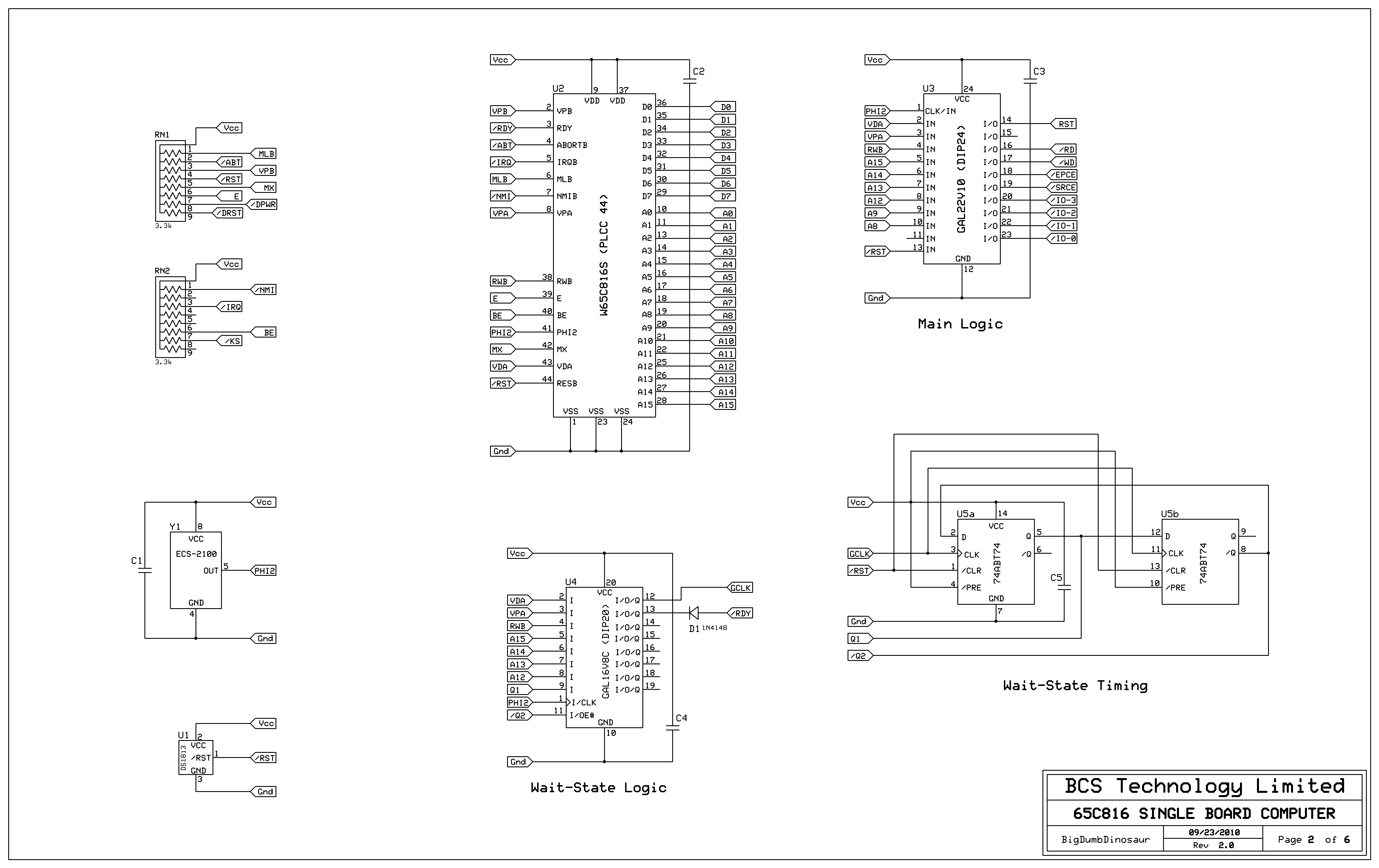
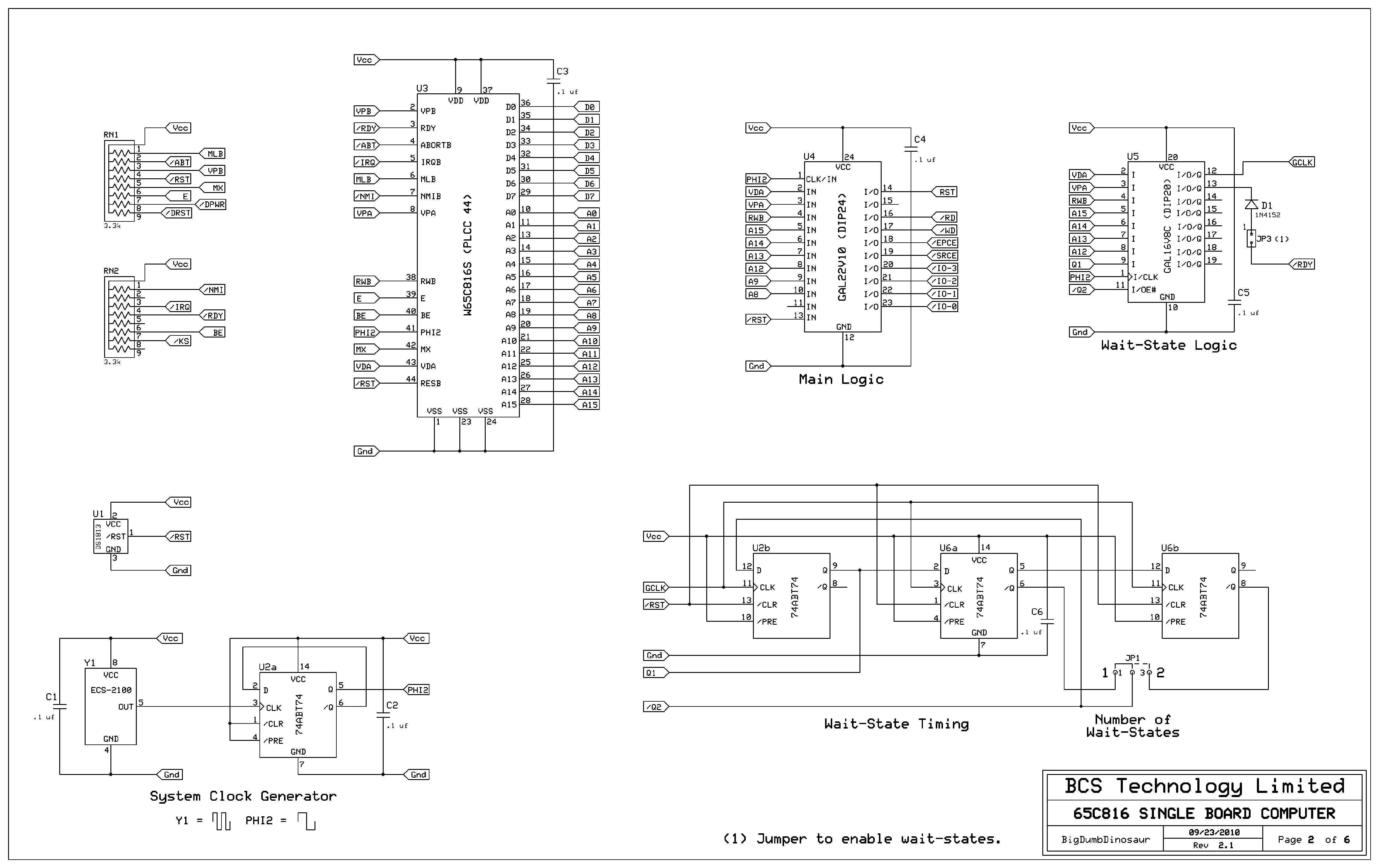
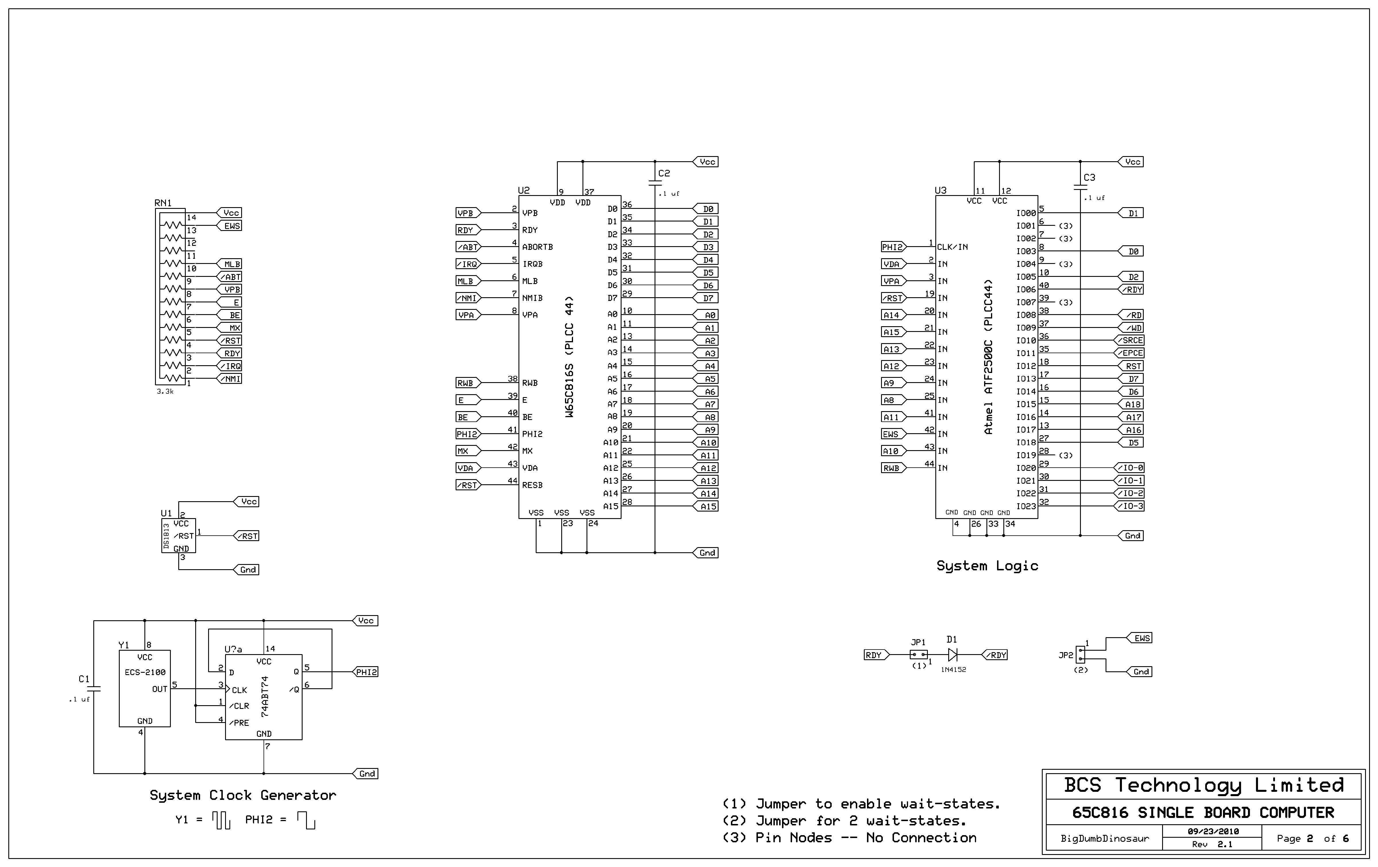
This new version uses a 22V10C GAL to replace the 74xx glue logic in the first unit, and also implements wait-stating when I/O hardware or ROM is accessed. The wait-state logic is handled by a second GAL (16V8C) and a dual 74ABT74 C-D flip-flop. Since the gate delays imposed by the old logic have been eliminated and wait-stating is now available, higher speeds should be possible than before. I'm going to try for a 20 MHz Ø2 clock this time around.
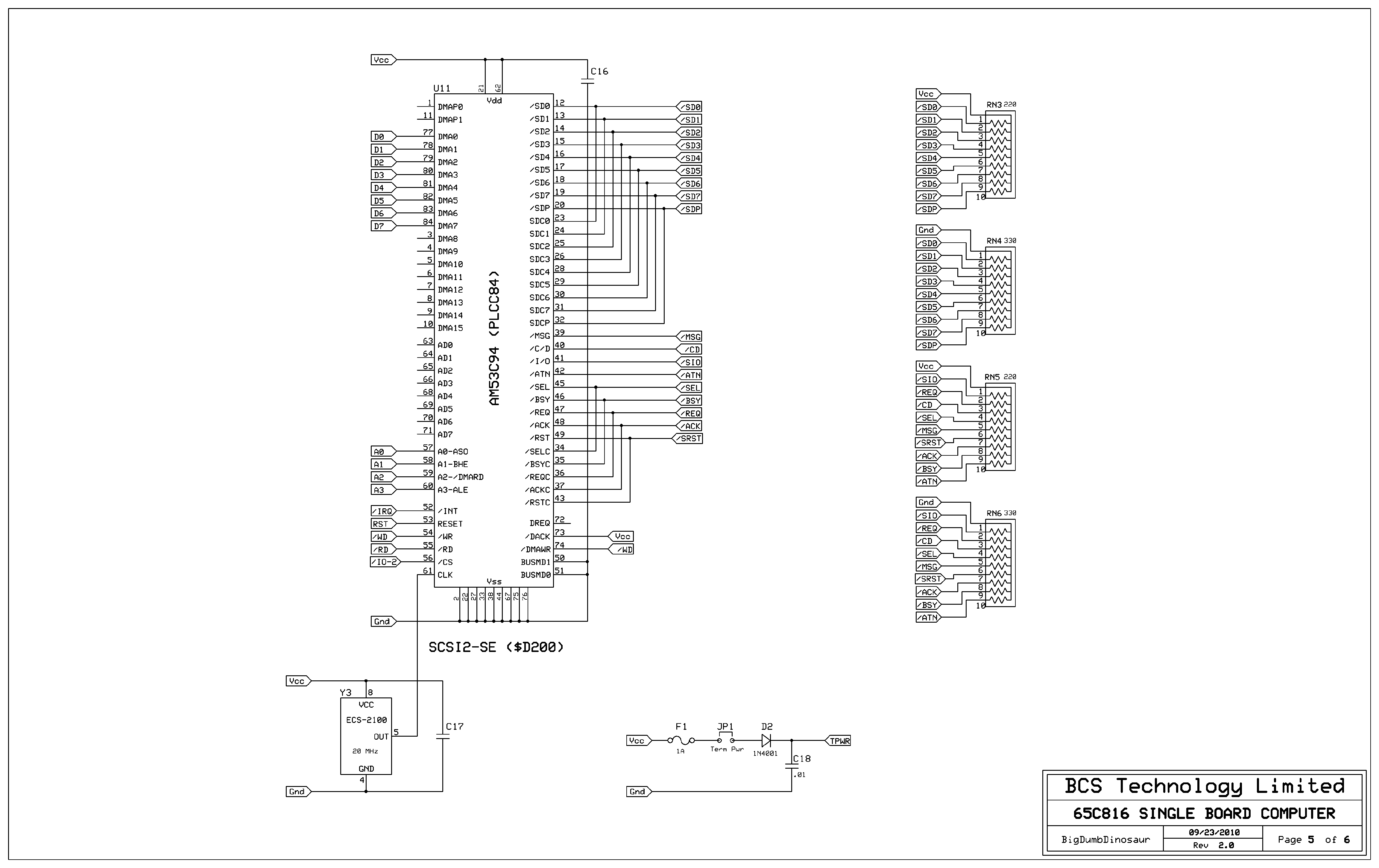
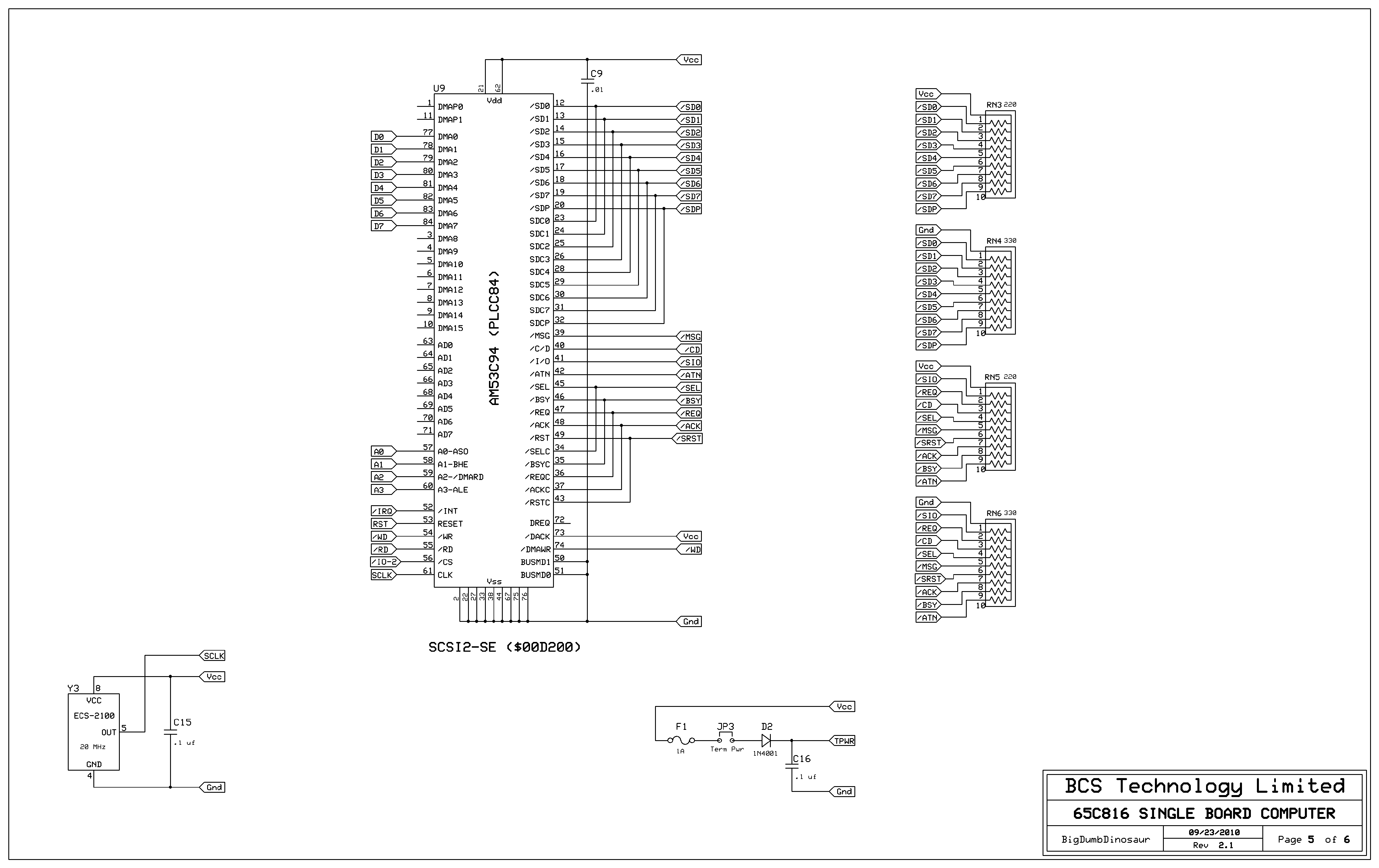
Also in this new design is a SCSI-SE port, driven by a 53C94 intelligent SCSI controller. The 'C94 is able to execute SCSI bus protocol sequences in hardware, thus offloading a considerable amount of work from the MPU. Without having to manipulate the SCSI bus signals in software, relatively simple (?) interrupt-driven code can be used to access SCSI devices. The 'C94 can be rigged up to run in PIO or DMA mode—I'm implementing PIO in this design due to not having a suitable DMA controller.
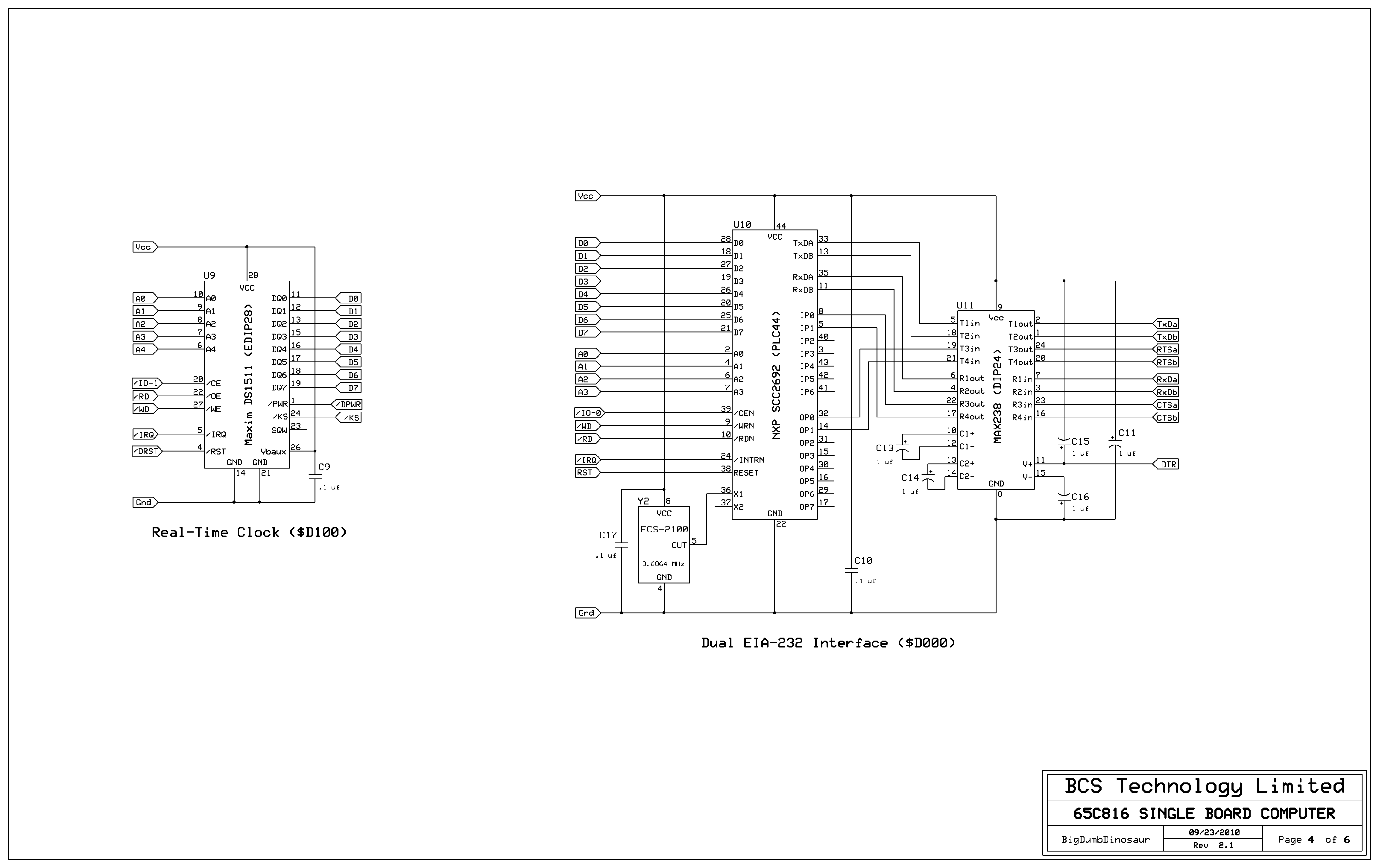
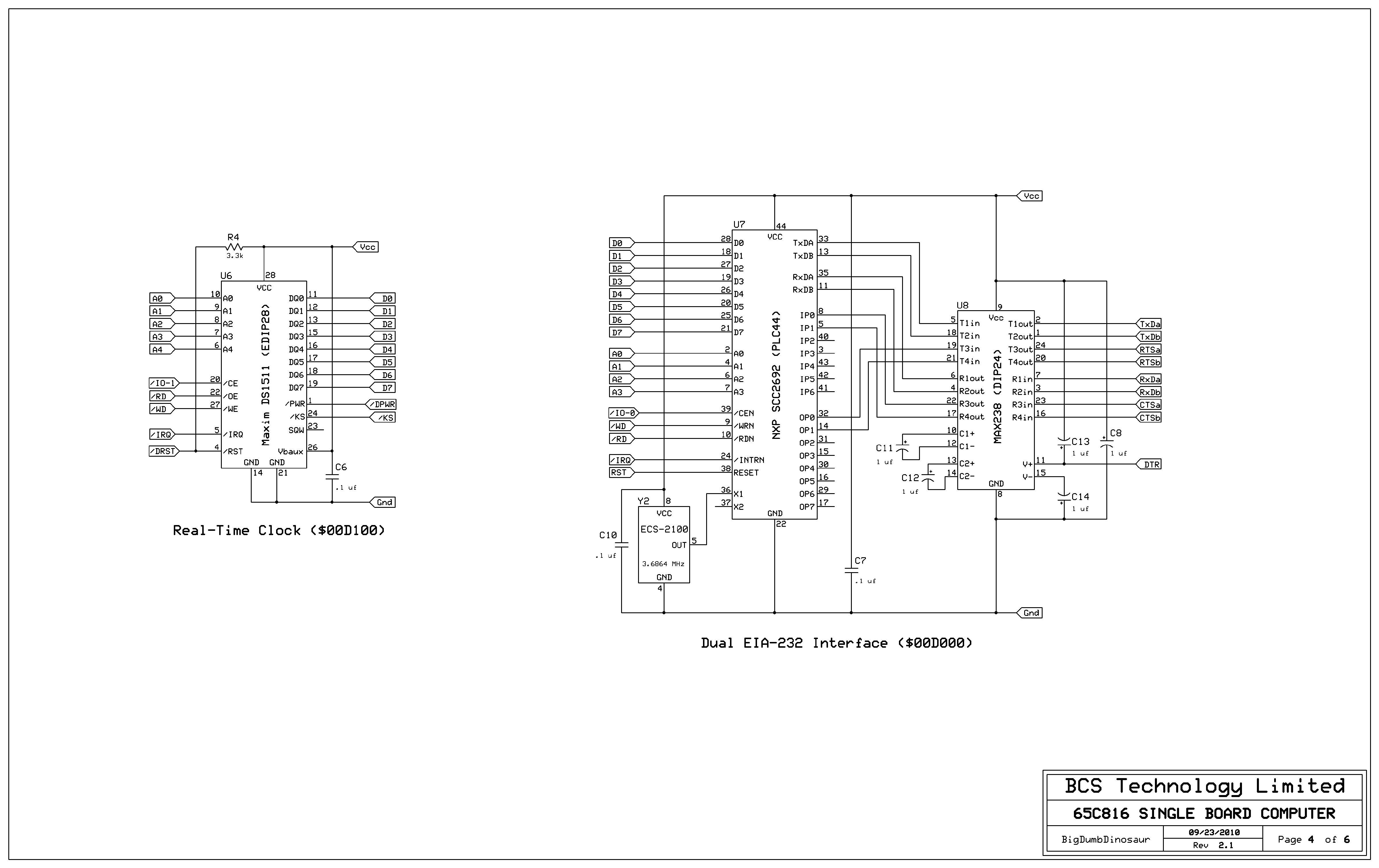
As with the POC V1 unit, POC V2.0 includes a dual 2692A ACIA for EIA-232 I/O and a Maxim (Dallas) DS1511 real time clock and watchdog timer.
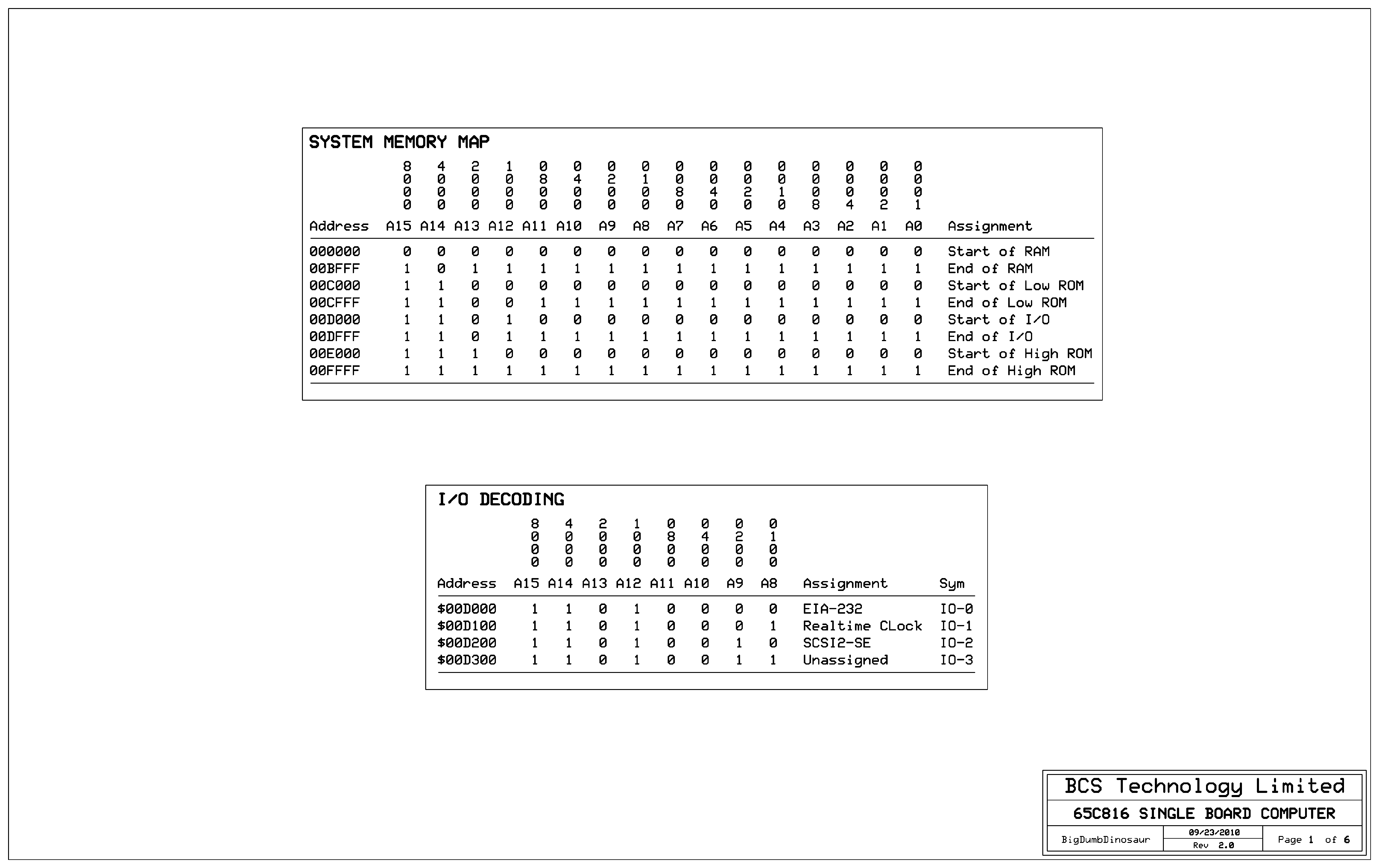
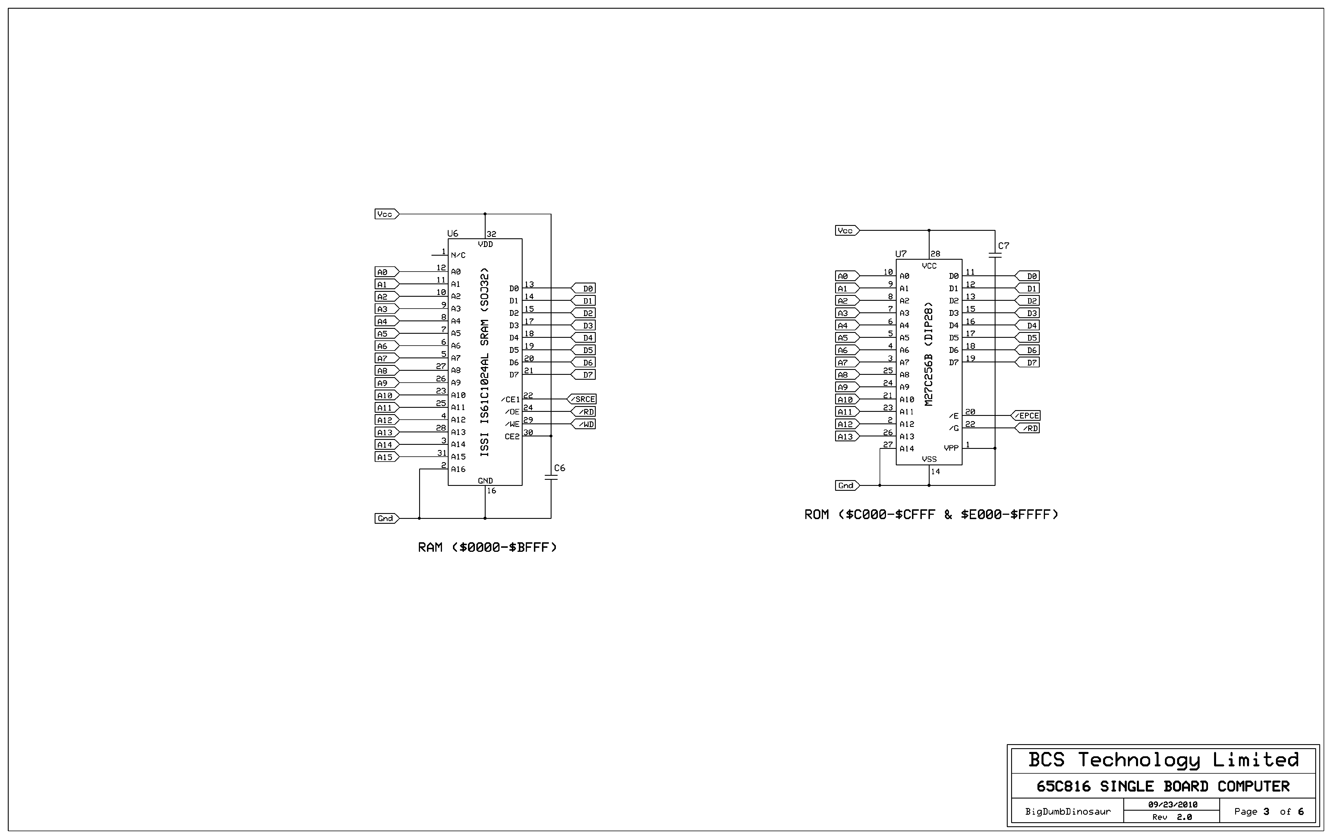
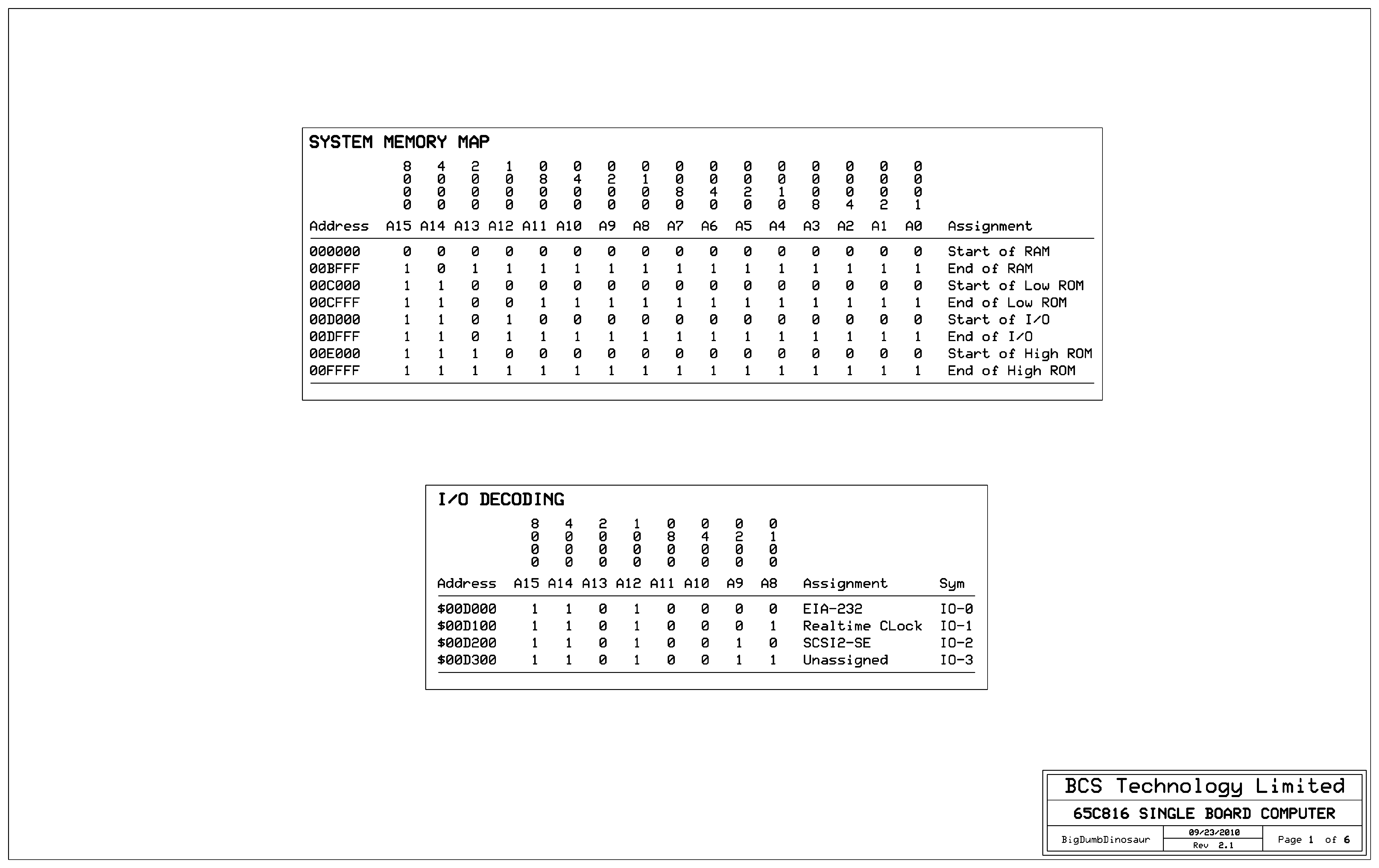
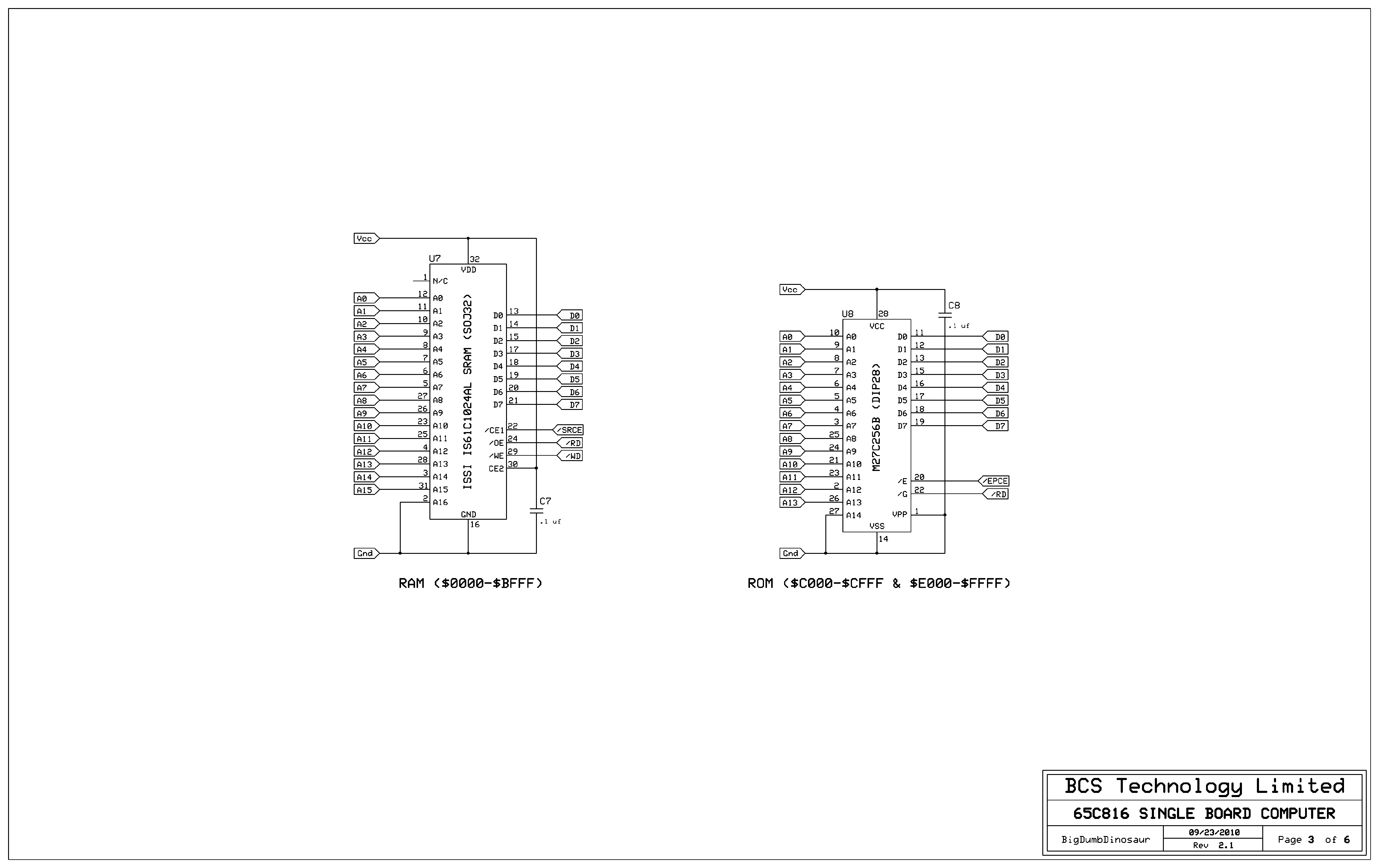
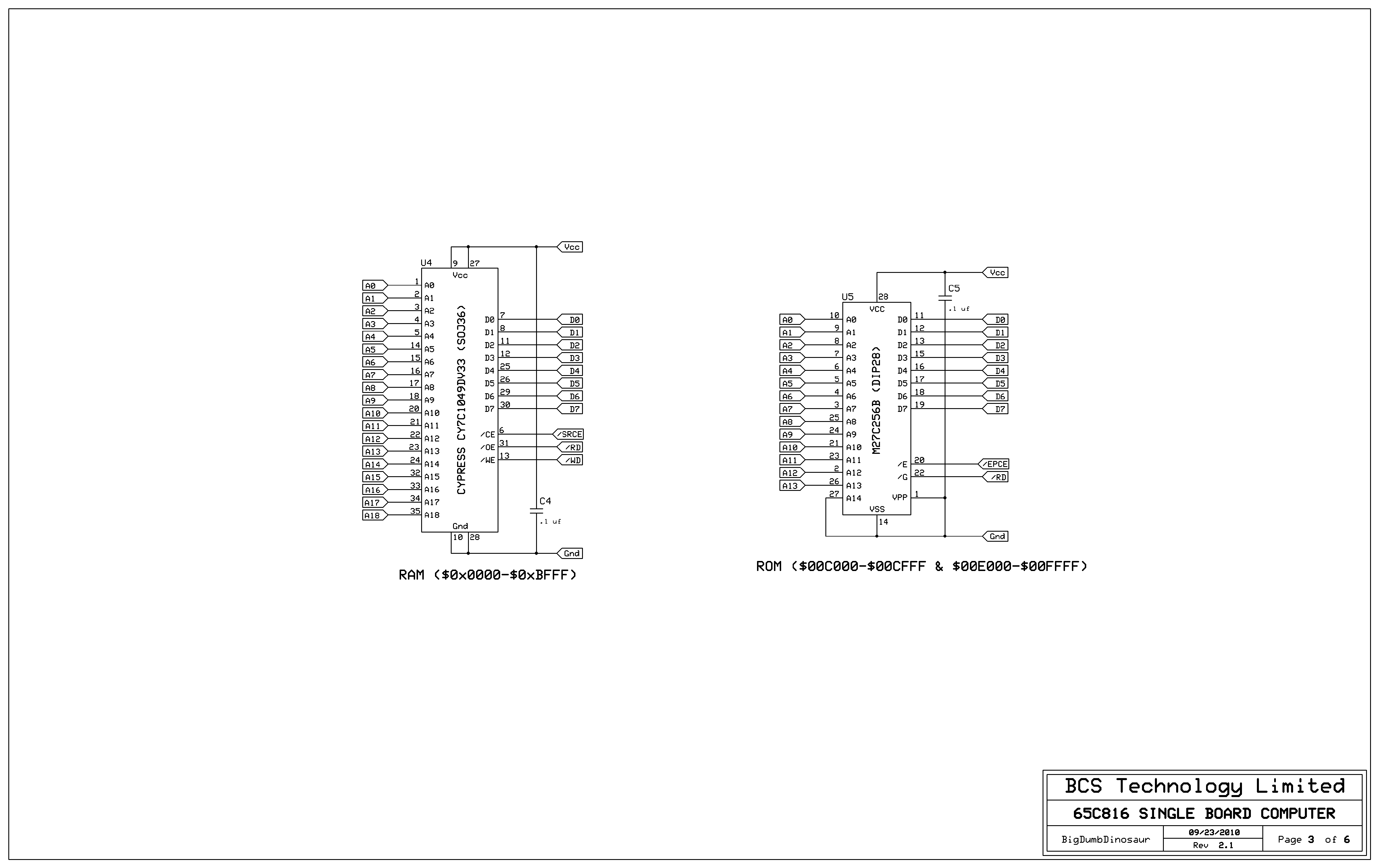
POC V1 had contiguous RAM from $0000 to $CFFF—implemented in 12 ns SRAM—and I/O at $D000, leaving 8K for the ROM. This version will reduce RAM to 48K, topping out at $BFFF, a change made necessary to get more room in the ROM to add the SCSI API. Hence ROM will be split into two sections, one at $C000-$CFFF and the other starting at $E000. The machine language monitor will be moved to the $C000 block to open up space in the $E000 block.
Here are the schematics:
Memory Map & I/O Assignments
Microprocessor Interface
RAM & ROM
Real Time Clock & EIA-232 Interface
SCSI-SE Interface
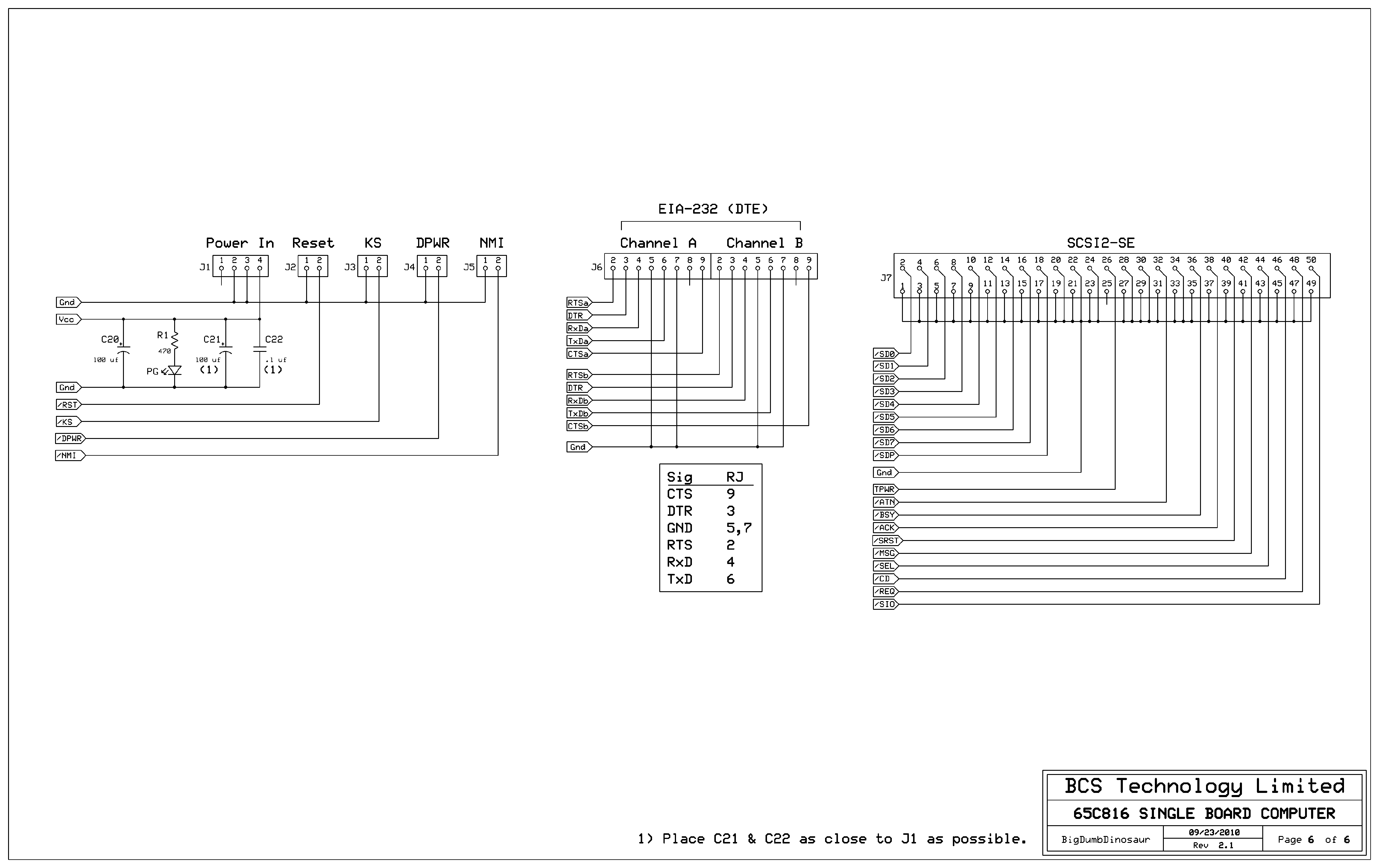
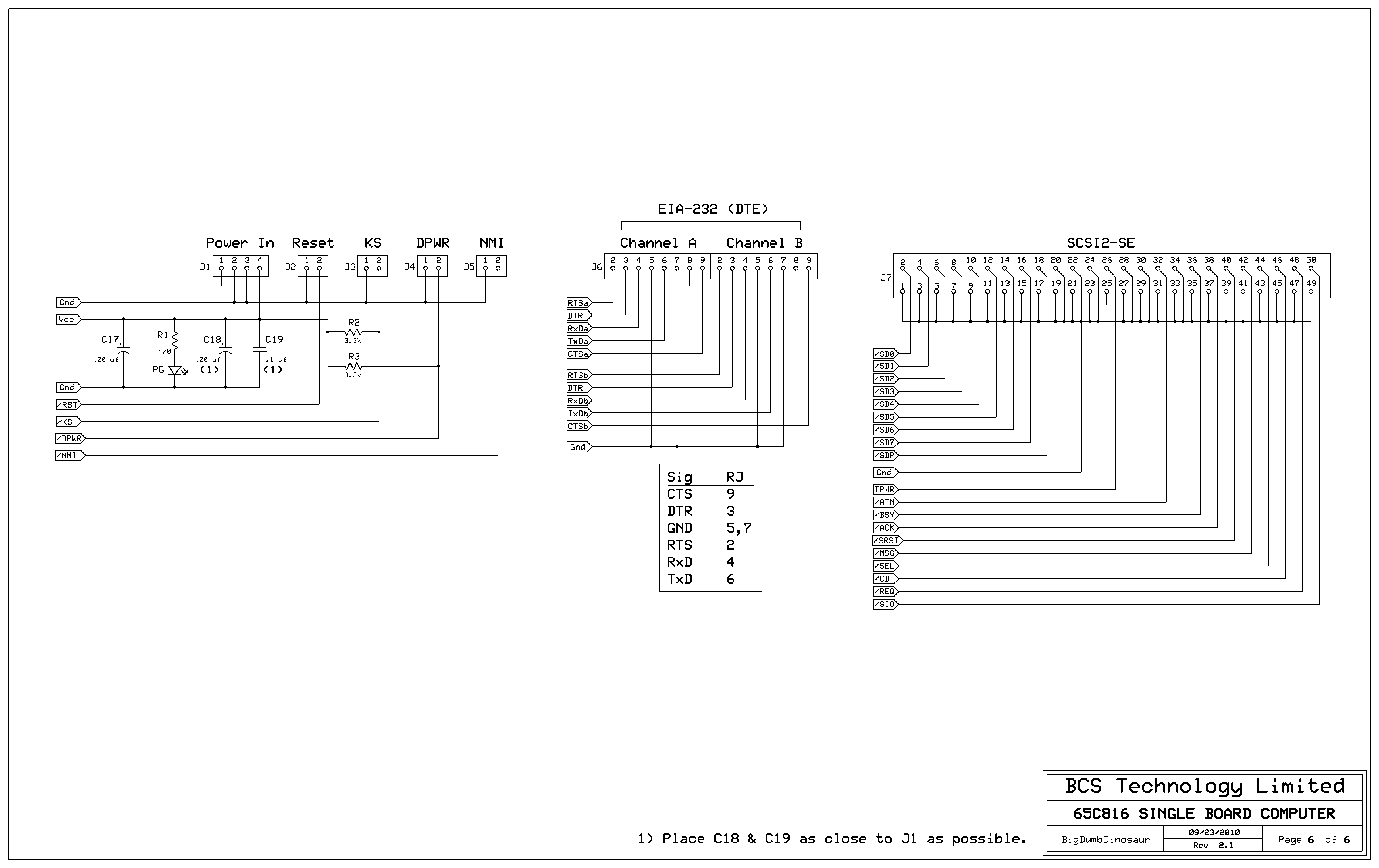
External Interface
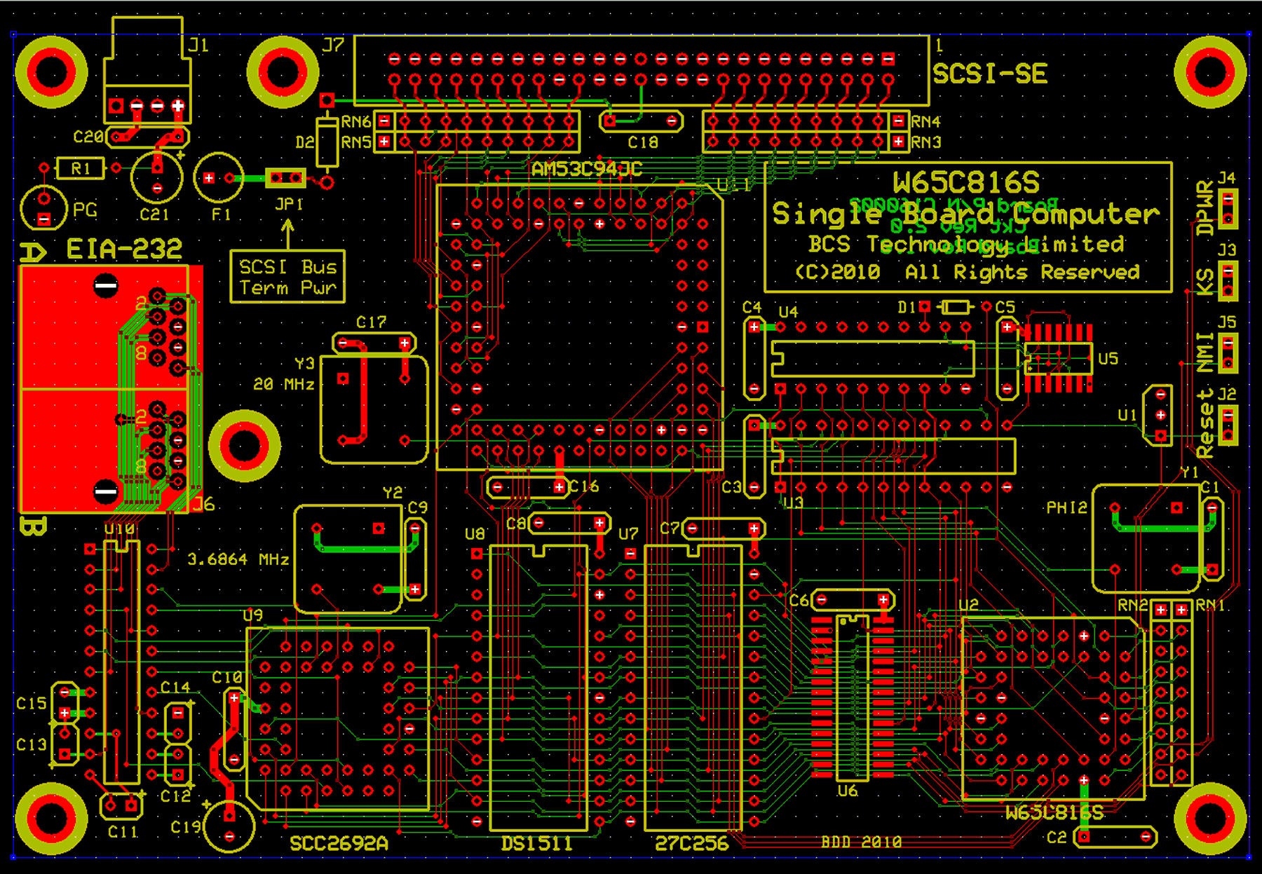
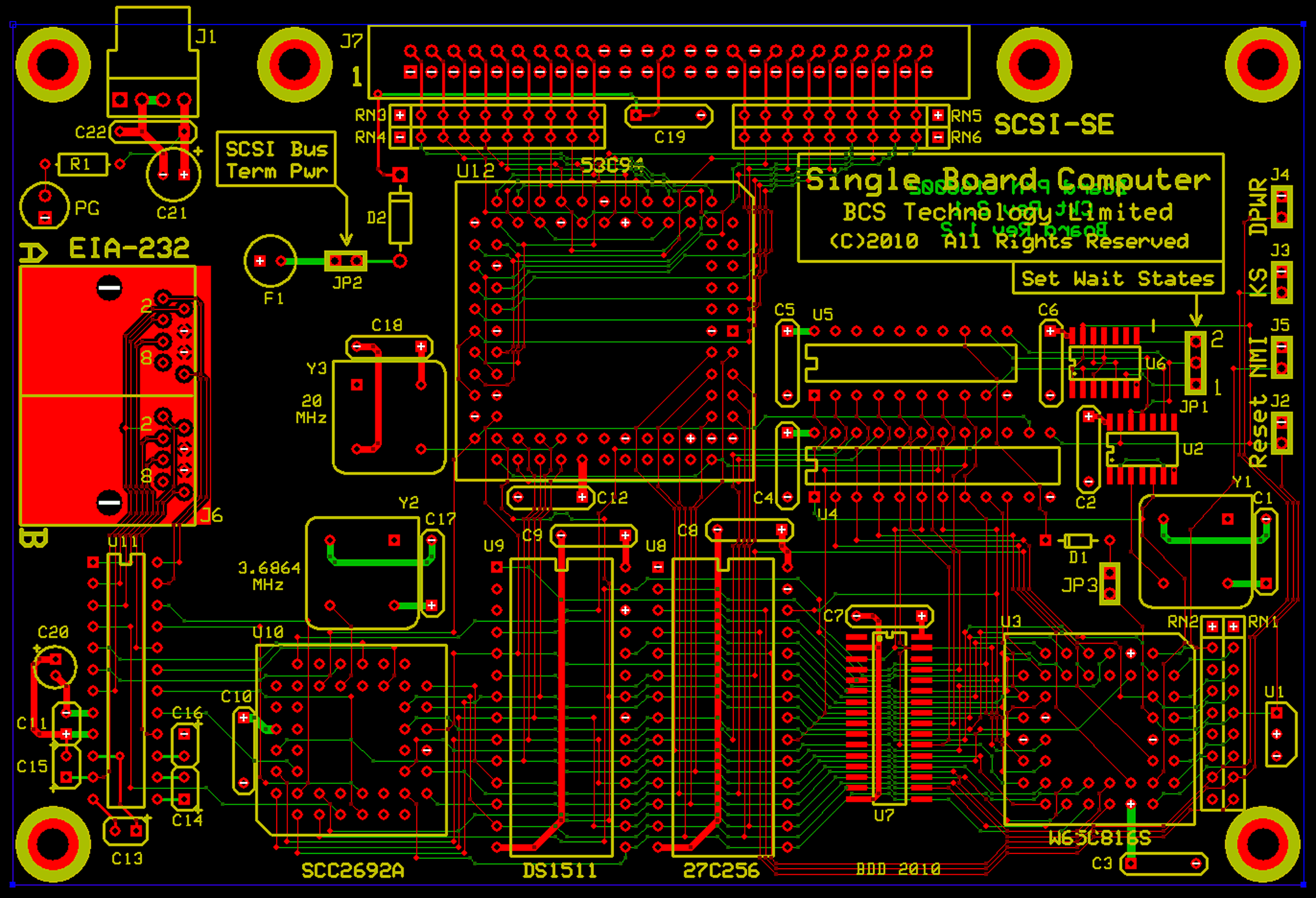
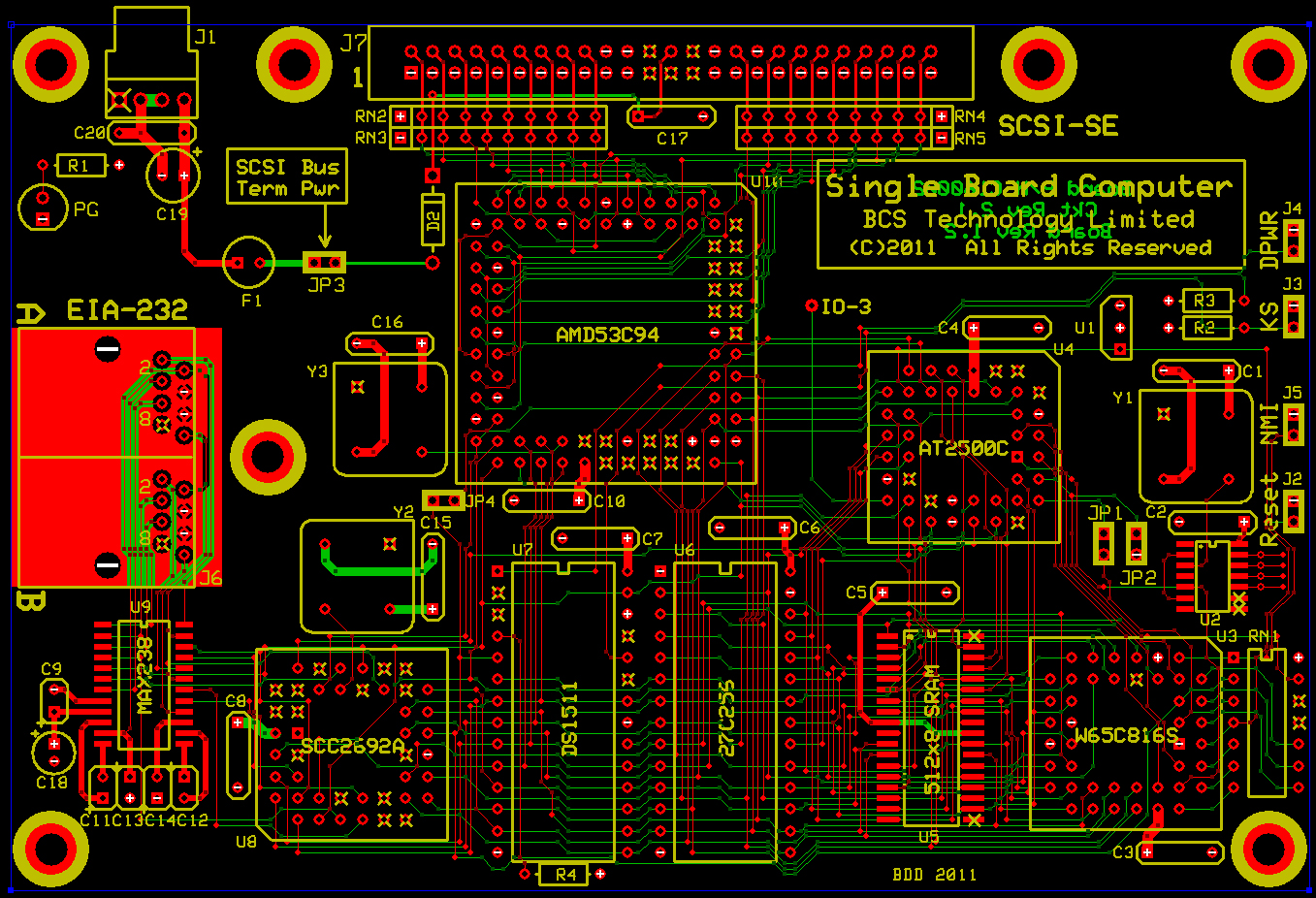
In redoing the printed circuit board layout, I decided to stick with the six inch width of the first version and increase the height to four inches to accommodate the SCSI hardware. I was going to try to squeeze the entire layout into 21 square inches (3.50 inch board height) to take advantage of ExpressPCB's ProtoPro service. However, ProtoPro has a limit of 650 holes per board and even though I eliminated some holes by not having all those PDIP packages that used to constitute the glue logic, I couldn't stay within that limit. Between the 53C94, the 50 pin SCSI receptacle and the SCSI bus termination resistors, 174 holes were added, putting the layout some 50 holes too high—and that didn't even account for extra via needed to connect everything. I considered directly soldering the 53C94 to the board on SMT pads, but thought better of it—how would I remove it if the design didn't work right? So this layout will use EPCB's production service.
Printed Circuit Board Layout
With this unit, I will now have the capability to implement some kind of operating system over and above the ROM code, due to mass storage being available. Once I've verified that the hardware is working, I'll have to get busy writing a SCSI API that can do simple tasks, such as device inquiry, read long, write long and request sense. Device inquiry will initially be the most useful, as it can prove out several aspects of the API, not the least of which would be the ability to read and write on the bus. Doing all this should keep me out of mischief for a while.
————————————————————
Edit #1: my typing basically sucks tonight...
Edit #2: POC V1 manages to run on a 15 MHz Ø2 clock. Dunno why, as none of the I/O hardware is rated for a 67 ns cycle time.

